Light-emitting diode package

A technology of light-emitting diodes and encapsulation layers, applied in electrical components, electrical solid-state devices, circuits, etc.

Active Publication Date: 2019-06-28
IND TECH RES INST
View PDF9 Cites 4 Cited by
  • Summary
  • Abstract
  • Description
  • Claims
  • Application Information

AI Technical Summary

Problems solved by technology

The shading layer is loc

Method used


Image

  • Light-emitting diode package
  • Light-emitting diode package
  • Light-emitting diode package

Examples


Embodiment Construction

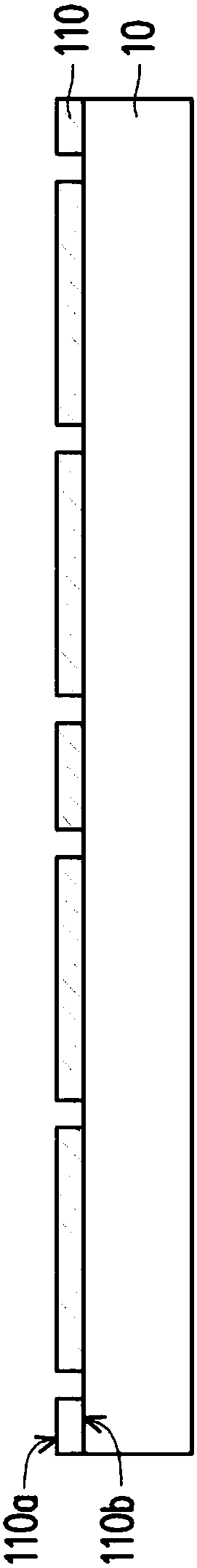
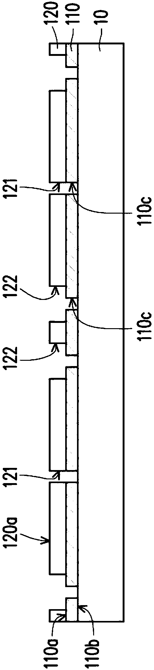
[0053] Figure 1A to Figure 1J It is a schematic cross-sectional view of the manufacturing method of the light emitting diode package according to the first embodiment of the present invention. Figure 1K It is a schematic top view of the light emitting diode package of the first embodiment of the present invention. Figure 1L It is a schematic bottom view of the light emitting diode package of the first embodiment of the present invention. Figure 1M It is a circuit diagram of the light emitting diode package of the first embodiment of the present invention.

[0054] First, please refer to Figure 1A , Provide a temporary carrier board 10. The material of the temporary carrier 10 can be glass, quartz, wafer, organic polymer, metal, etc. Other suitable materials can also be used as the temporary carrier board 10, as long as the aforementioned materials can support the film layer or member formed thereon and can withstand the subsequent manufacturing process, which is not limited in...


PUM

PropertyMeasurementUnit
Young's modulusaaaaaaaaaa

Abstract

The invention discloses a light-emitting diode package which comprises a line layer, a light shielding layer, a plurality of light-emitting diodes and a packaging layer. The thickness of the line layer is smaller than 100 micrometers. The light shielding layer is on the line layer. The light shielding layer has multiple openings. The light emitting diodes are configured on the line layer and in the openings of the light shielding layer. The light emitting diodes are electrically connected with the line layer. The packaging layer covers the light shielding layer. The refractivity of the packaging layer is 1.4-1.7. The Young's modulus of the packaging layer is higher than or equal with 1GPa. The thickness of the packaging layer is higher than that of the light emitting diode.

Description


Claims


Application Information

Patent Timeline
Owner IND TECH RES INST
Why Eureka
Try Eureka