Light-emitting device and method for manufacturing the same

a technology of light-emitting devices and manufacturing methods, which is applied in the direction of semiconductor devices, electrical devices, layered products, etc., can solve the problems of insufficient luminous efficiency of this type of light-emitting devices, difficult to emit the light generated within the element to the outside, and large loss of luminous energy by reflection, etc., to achieve rapid loss of rough surface structure and good economical performance

Inactive Publication Date: 2005-05-26
AGILENT TECH INC
View PDF7 Cites 267 Cited by
  • Summary
  • Abstract
  • Description
  • Claims
  • Application Information

AI Technical Summary

Benefits of technology

[0041] The same argument is valid with respect to the height of the projections. Since the size of the roughened surface structure of the invention is smaller than the light wavelength, the light senses the mean value of the size of the roughened surface structure instead of sensing respective sizes of the projections in the structure. Accordingly, the refractive index that is sensed by the light corresponds to a mean refractive index on the surface parallel to the light-emitting surface, when a light emitting layer having a higher refractive index and a medium having a lower refractive index exist together. It is desirable that the mean value of the refractive index is smoothly decreased from the light emitting layer until the light reaches the outside of the element. For obtaining such gradient of the refractive index, it is desirable that the top and bottom levels of the roughened surface structure, or the height of the projections, are distributed to a certain extent, rather than they are perfectly uniform. In the structure of the surface of the light-emitting element, it is necessary that the mean height <H> of the projections in the roughened surface structure (<H>=ΣH2nH/ΣHnH) is larger than {fraction (1/10)} of the light wavelength and smaller than the light wavelength, and that the dispersion σH of the height (σH=<H>/(ΣHnH/ΣnH)) is 1.05 or more and 2 or less. The shape of the roughened surface structure is desirably approximated by a circular cone for obtaining a gradient of the refractive index.
[0042] The mean height <H> of projections is defined by a mean-square height for weighting since the response of the light is larger as the size of the surface roughness is larger.
[0043] The mean height <H> of projections is desirably {fraction (1/10)} or more of the light wavelength. When the mean height <H> of projections is smaller than {fraction (1/10)}, the refractive index changes within a very short distance, and the effect of the gradient of the refractive index is lost by the same principle as described above with respect to the radius of g

Problems solved by technology

Refractive indices of compound semiconductors constituting light-emitting devices are so high that much luminous energy is lost by reflection at the surface and interface of most of the light-emitting devices and the like.
Therefore, it is difficult to emit the light generated within the element to outside.
However, luminous efficiency is yet insufficient in this type of light-emitting device due to a relatively large refractive index difference between the light-emitting surface and the monolayer film.
However, since it is almost the limit of photolithography even by using a lat

Method used


Image

  • Light-emitting device and method for manufacturing the same
  • Light-emitting device and method for manufacturing the same
  • Light-emitting device and method for manufacturing the same

Examples


example 1

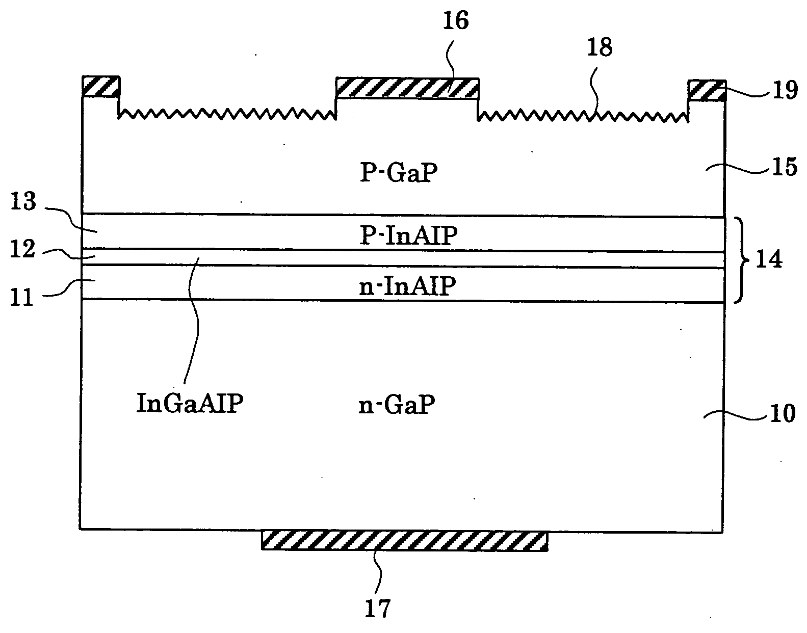
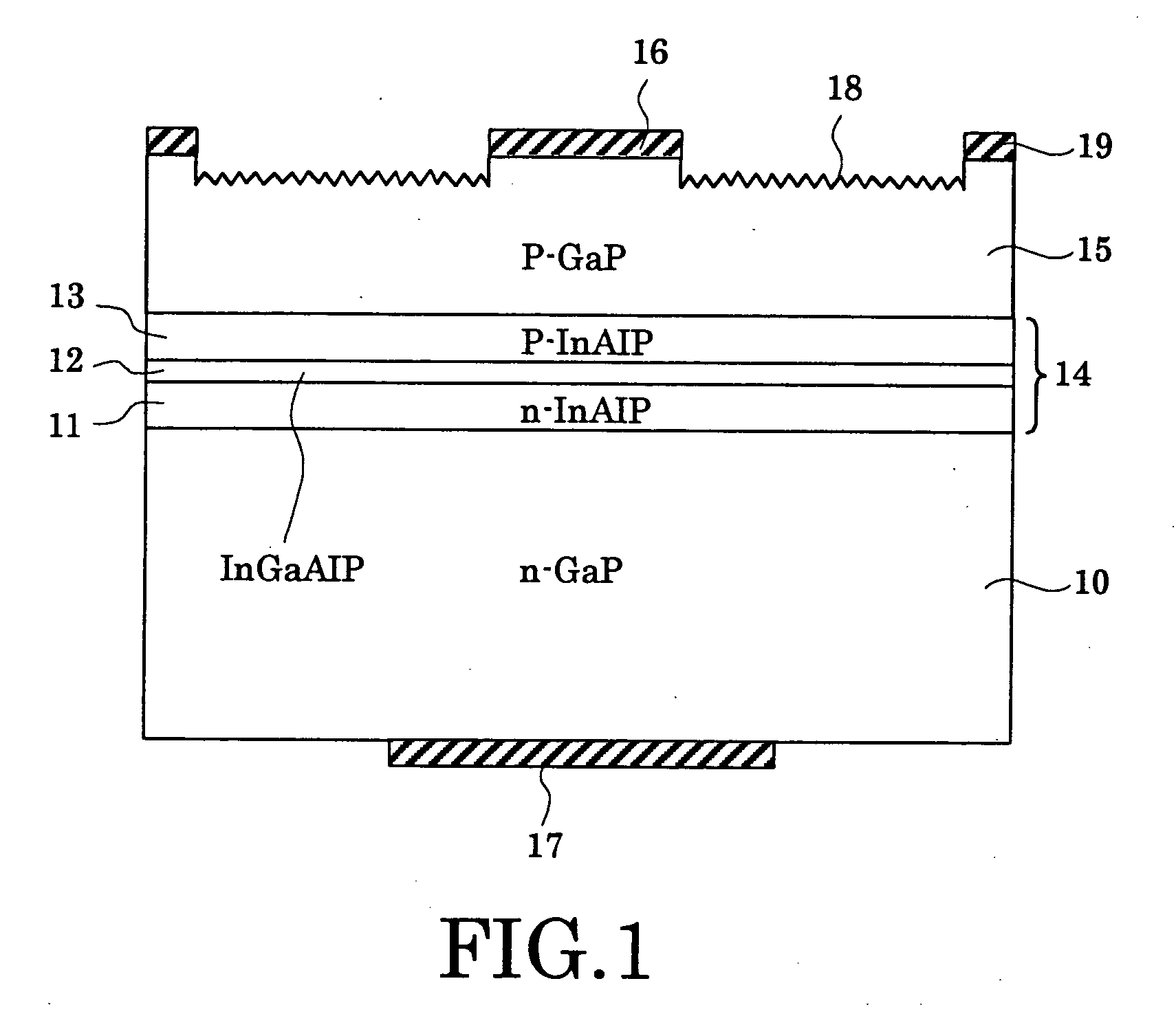
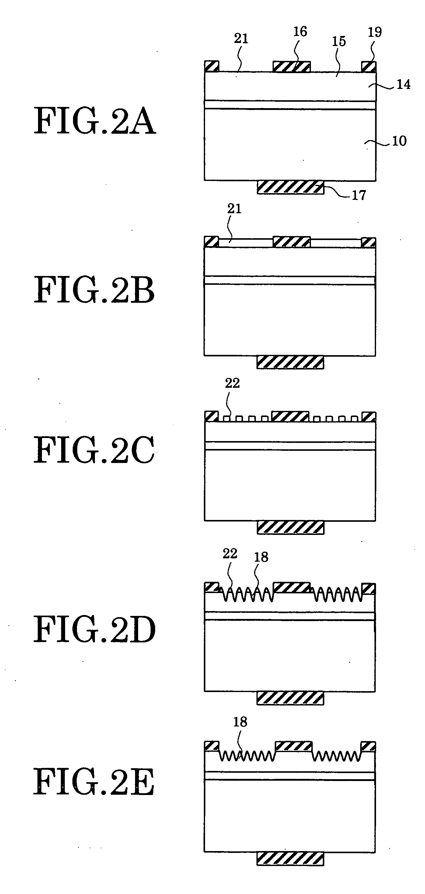
[0118] Examples of the invention will be described with reference to the drawings. As shown in FIG. 2-1, the a GaAs or GaP compound semiconductor substrate 10 comprises an electrode 17 on one surface (bottom surface), and a light emitting layer 14 and a current diffusion layer 15 are epitaxially grown on the other surface of the substrate with an electrode 16 and an electrode wiring pattern 19 on the current diffusion layer. A n-GaAs, n-GaP or p-GaP is used for the semiconductor substrate, and an n-InAlP or p-InAlP cladding layer, an InGaAlP active layer and a light emitting layer are formed as a hetero-multilayer structure on the substrate. A p-InAlP, p-GaP or n-InGaAlP current diffusion layer 15 is laminated on the light emitting layer.

[0119] After applying a solution prepared by dissolving a block copolymer in a solvent on the substrate of the light-emitting element by spin-coating at a rotation number of 2500 rpm, the solvent was evaporated by pre-baking at 110° C. for 90 secon...

example 2

[0122] A substrate with the block copolymer after phase separation by the same method as in Example 1 was etched by RIE under the condition of an O2 flow speed of 30 sccm, an etching gas pressure of 13.3 Pa (100 mTorr) and an etching power of 100w to etch the separated PS and PMMA phases. Although O2 cannot etch the substrate like CF4, the PMMA phase can be selectively etched clearly. The process as in Example 1 was applied thereafter, thereby obtaining the same pattern as in Example 1. The fine roughened pattern comprises a mean diameter 2 of projections of about 60 nm with σR of 1.2, a repeating cycle of projections of about 100 nm, and a mean height of projections of about 110 nm with σH of 1.4. The substrate was processed into an element and was subjected to a surface treatment, and the element was compared with a light emitting diode with no surface processing, finding that luminance showed 21% of improvement as an average of 10 devices.

example 3

[0123] A block copolymer comprising PS with a molecular weight of 315,000 and PMMA with a molecular weight of 785,000 was dissolved in a solvent. The solution was applied on the surface of the light emitting layer of the GaP substrate as the light emitting diode used in Example 1 by spin coating at a rotation number of 3000 rpm. The solvent in the applied layer was evaporated by pre-baking at 110° C. for 90 minutes, thereby obtaining a layer with a thickness of 150 nm. The layer was then annealed at 210° C. for 4 hours to separate the PS and PMMA phases with each other, thereby forming a dot pattern of PS with a diameter of each dot of about 110 nm. The GaP substrate with the block copolymer after phase separation was etched by RIE under the condition of an O2 flow speed of 30 sccm, an etching gas pressure of 13.3 Pa (100 mTorr) and an etching power of 100W to etch the separated PS and PMMA phases. Although the GaP substrate is not etched with O2, the PMMA phase is selectively etche...


PUM


Abstract

A nanometer size roughened structure is formed on a surface of a light-emitting element, and luminous efficiency is improved. The roughened structure on the surface of the light-emitting element of the invention is formed into the following shape such that the refractive index smoothly changes: (1) the mean diameter of projections on the roughened surface is smaller than the light wavelength; (2) a pitch of the roughened surface is irregular; and (3) positions of the top and bottom of the roughened surface are distributed from their mean values within the light wavelength in order to give a smooth gradient of the refractive index. The surface of such light-emitting element is obtained by forming a thin film on the surface of the light-emitting element using a resin composition which contains a block copolymer or graft copolymer and forms a micophase-separated structure in a self-organization manner; selectively removing at least one phase of the microphase-separated structure of the thin film formed on the surface; and etching the surface of the light-emitting element using the remaining phase as an etching mask.

Description

CROSSREFERENCE TO RELATED APLICATION [0001] This application is based upon and claims the benefit of priority from the prior Japanese Patent Application No. 2001-402004, filed on Dec. 28, 2001; the entire contents of which are incorporated herein by reference. BACKGROUND OF THE INVENTION [0002] 1. Field of the Invention [0003] The present invention relates to a light-emitting device that is able to realize a high luminous efficiency by emitting a light generated in a light-emitting element with a high efficiency, and a method for manufacturing the same. [0004] 2. Description of the Related Art [0005] Refractive indices of compound semiconductors constituting light-emitting devices are so high that much luminous energy is lost by reflection at the surface and interface of most of the light-emitting devices and the like. Therefore, it is difficult to emit the light generated within the element to outside. For example, since the compound semiconductor such as gallium phosphide (GaP) ha...

Claims


Application Information

Patent Timeline
IPC IPC(8): H01L33/22
CPCH01L33/22H01L21/0271
Inventor ASAKAWA, KOJIFUJIMOTO, AKIRASUGIYAMA, HITOSHIOHASHI, KENICHISUZUKI, KENJITONOTANI, JUNICHI
Owner AGILENT TECH INC
Why Eureka
Try Eureka