Supercharge Your Innovation With Domain-Expert AI Agents!

Power domain switch control circuit and method and chip

A switch control circuit and switch control technology, applied in electronic switches, data processing power supplies, electrical components, etc., can solve problems such as large-amplitude instantaneous current pulses, device breakdown, etc., and achieve the effect of improving reliability and reducing power consumption

Active Publication Date: 2019-07-12
JIANGSU XINSHENG INTELLIGENT TECH CO LTD
View PDF3 Cites 1 Cited by
  • Summary
  • Abstract
  • Description
  • Claims
  • Application Information

AI Technical Summary

Problems solved by technology

In such a small time difference, all the driving devices in the power domain are turned on one after another. At the moment when all the driving devices are powered on and off at the same time, due to the leakage current, an instantaneous current pulse with a large amplitude will be generated, resulting in the risk of breakdown of some devices.

Method used


Image

  • Power domain switch control circuit and method and chip
  • Power domain switch control circuit and method and chip
  • Power domain switch control circuit and method and chip

Examples


Embodiment Construction

[0042] The following will clearly and completely describe the technical solutions in the embodiments of the application with reference to the drawings in the embodiments of the application. Apparently, the described embodiments are only some of the embodiments of the application, not all of them. Based on the embodiments in this application, all other embodiments obtained by persons of ordinary skill in the art without making creative efforts belong to the scope of protection of this application.

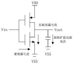
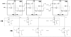
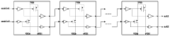
[0043] In the prior art, the turn-on time difference of all driving devices in the power domain is extremely small, which generates a large instantaneous current pulse, which may cause some devices to be broken down. In this application, the control of the drive device is controlled by two enable signals separated by a preset time delay, thereby avoiding the generation of excessive current transient pulses and protecting the internal devices of the chip.

[0044] The embodiment of t...


PUM


Abstract

The invention discloses a power domain switch control circuit and method and a chip, the power domain switch control circuit comprises N PSWs, a first enable signal and a second enable signal are respectively accessed to a first input end and a second input end of a first PSW, and a first input end and a second input end of an ith PSW are respectively connected with the first output end and the second output end of the i-1th PSW and the first output end and the second output end of the Nth PSW respectively output a first confirmation signal and a second confirmation signal; wherein the first enable signal and the second enable signal are separated by a preset time delay, each PSW comprises a first switch unit and a second switch unit, and the first input end and the second input end are respectively used for controlling the on-off state. Therefore, on-off of the first switch unit controlled by the first enable signal and on-off of the second switch unit controlled by the second enablesignal do not interfere with each other, action time difference exists, overlarge current instantaneous pulse generated by simultaneous on-off is avoided, and internal devices of the chip are protected.

Description

technical field [0001] The present application relates to the technical field of chip design, in particular to a power domain switch control circuit, method and chip. Background technique [0002] The research on low power consumption of chips is usually based on the transistor level, starting from the analysis of the source of power consumption. The power consumption of CMOS (Complementary Metal Oxide Semiconductor, Complementary Metal Oxide Semiconductor) usually includes three parts, one is the dynamic power consumption caused by charging and discharging the load capacitor; The tubes are turned on at the same time to form a short-circuit current between the power supply and the ground, resulting in short-circuit power consumption, and the third is static power consumption caused by leakage current. Such as figure 1 As shown, the leakage current here mainly includes: gate leakage current, sub-threshold current and drain diffusion junction leakage current. [0003] In ex...

Claims


Application Information

Patent Timeline
Patent Type & Authority Applications(China)
IPC IPC(8): H03K17/687G06F1/26
CPCH03K17/687G06F1/266H03K2217/0081
Inventor 张亮
Owner JIANGSU XINSHENG INTELLIGENT TECH CO LTD
Features
  • R&D
  • Intellectual Property
  • Life Sciences
  • Materials
  • Tech Scout
  • Unparalleled Data Quality
  • Higher Quality Content
  • 60% Fewer Hallucinations
Learn More