Safe password chip testability design structure in boundary scanning design environment

A technology of boundary scan and design structure, which is applied to secure communication devices and key distribution, can solve the problems of not finding patented inventions of cryptographic chips, etc., and achieve the effect of low area cost

Pending Publication Date: 2019-07-16
CHANGSHA UNIVERSITY OF SCIENCE AND TECHNOLOGY
View PDF7 Cites 3 Cited by
  • Summary
  • Abstract
  • Description
  • Claims
  • Application Information

AI Technical Summary

Problems solved by technology

[0005] In the existing patents, no patented invention similar to the testability design str

Method used


Image

  • Safe password chip testability design structure in boundary scanning design environment
  • Safe password chip testability design structure in boundary scanning design environment
  • Safe password chip testability design structure in boundary scanning design environment

Examples


Embodiment Construction

[0026] The present invention will be described in detail below in conjunction with the drawings.

[0027] In order to make the objectives, technical solutions, and advantages of the present invention clearer, the following further describes the present invention in detail with reference to the accompanying drawings and embodiments. It should be understood that the specific embodiments described here are only used to explain the present invention, but not to limit the present invention.

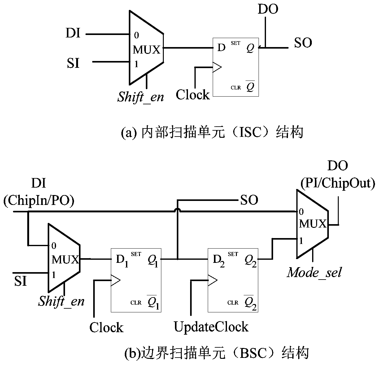
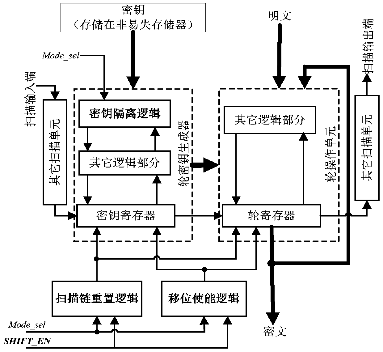
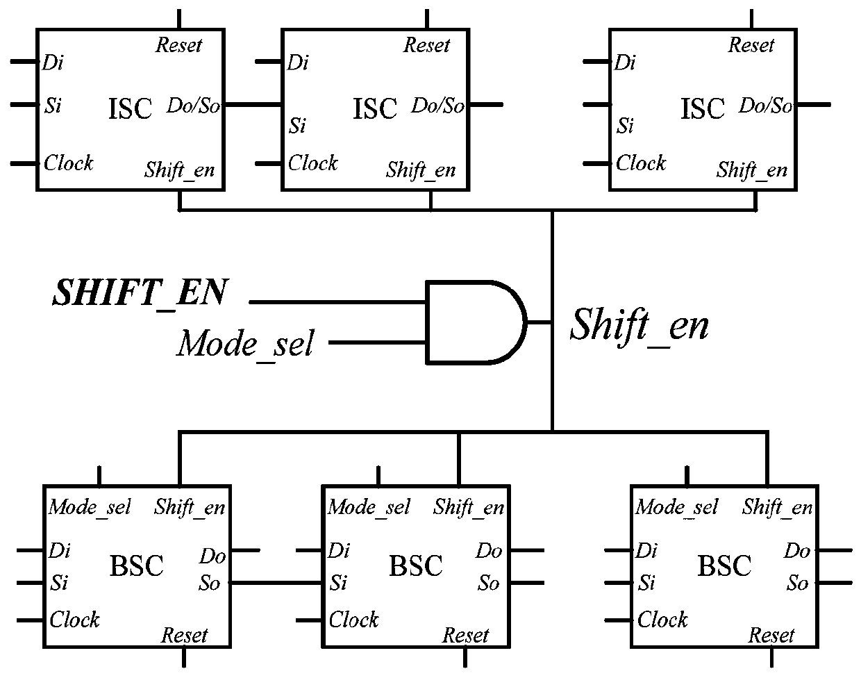
[0028] When using the technology of the present invention to protect the chip, the above-mentioned security control logic needs to be inserted in the chip design stage. After inserting the safety control logic, the working and testing process of the chip is as follows.

[0029] 1. After power-on, if the mode selection signal and shift enable signal {Mode_sel, SHIFT_EN} are both set to 0, the crypto chip runs in functional mode, and the initial key can be loaded into the key register to perform encry...


PUM


Abstract

The invention discloses a testability design structure for protecting an AES password chip from scanning attack in a boundary scanning design environment. According to the safe testability design structure, shift enable logic, scan chain mode switching reset logic and key isolation logic are introduced on the basis of a conventional boundary scan design structure. The shift enable logic is used for disabling a scanning shift operation in a functional mode; the scan chain mode switching reset logic enables the chip to execute a reset operation at first when switching from a function mode to a test mode, so that confidential information stored in the scan chain is protected; and the key isolation logic is used for isolating the encryption key in the test mode so as to prevent the attacker from obtaining the key information in the test mode. New input and output signals are not introduced, only little hardware expenditure is needed, the chip can be automatically protected, and all potential side channel attacks based on scanning can be resisted on the premise that the testability of the circuit is not damaged.

Description

Technical field [0001] The invention belongs to the field of chip security, and more specifically, relates to a security testability design structure for protecting cryptographic chips from scanning-based non-intrusion attacks. Background technique [0002] With the development of emerging technologies such as the Internet of Things and big data, information security and privacy have become more and more important, and cryptographic algorithms have been widely used. Since the data throughput rate provided by software implementation is low, and more computing resources are required, cryptographic algorithms are usually implemented by hardware modules. The encryption algorithm has zero tolerance to failure, so the encryption hardware needs to be strictly tested. [0003] Scanning design improves the controllability and observability of the internal triggers of the chip, and converts the test of sequential circuits into the test of combinational circuits, which brings great convenien...

Claims


Application Information

Patent Timeline
IPC IPC(8): G06F21/75H04L9/00H04L9/06H04L9/08
CPCG06F21/75H04L9/002H04L9/0631H04L9/0894
Inventor 王伟征王威蔡烁
Owner CHANGSHA UNIVERSITY OF SCIENCE AND TECHNOLOGY
Why Eureka
Try Eureka