
Semiconductor package

A semiconductor and packaging substrate technology, applied in the direction of semiconductor devices, semiconductor/solid-state device components, electric solid-state devices, etc., to achieve the effects of improving heat dissipation, reducing warpage, and improving mechanical strength

Inactive Publication Date: 2019-07-16
MEDIATEK INC
View PDF3 Cites 3 Cited by
  • Summary
  • Abstract
  • Description
  • Claims
  • Application Information

AI Technical Summary

Problems solved by technology

Heat dissipation becomes a challenge as die power consumption, die size and thermal density increase with each new generation of microprocessors

Method used


Image

  • Semiconductor package
  • Semiconductor package
  • Semiconductor package

Examples


Embodiment Construction

[0054] Specific terms are used throughout the specification and the following claims to refer to specific components. Manufacturers may refer to components by different names, as those skilled in the art will recognize. This document does not intend to distinguish between those components that have different names but have the same function. In the following description and claims, the terms "comprising" and "comprising" are used in an open-ended category and should therefore be construed to mean "including, but not limited to...". Also, the term "coupled" is intended to mean an indirect or direct electrical connection. Thus, if a device couples to another device, that connection may be a direct electrical connection or an indirect electrical connection via other devices and connections.

[0055]The following description is of the best contemplated mode of carrying out the invention. This description is intended to illustrate the general principles of the invention and not ...


PUM


Abstract

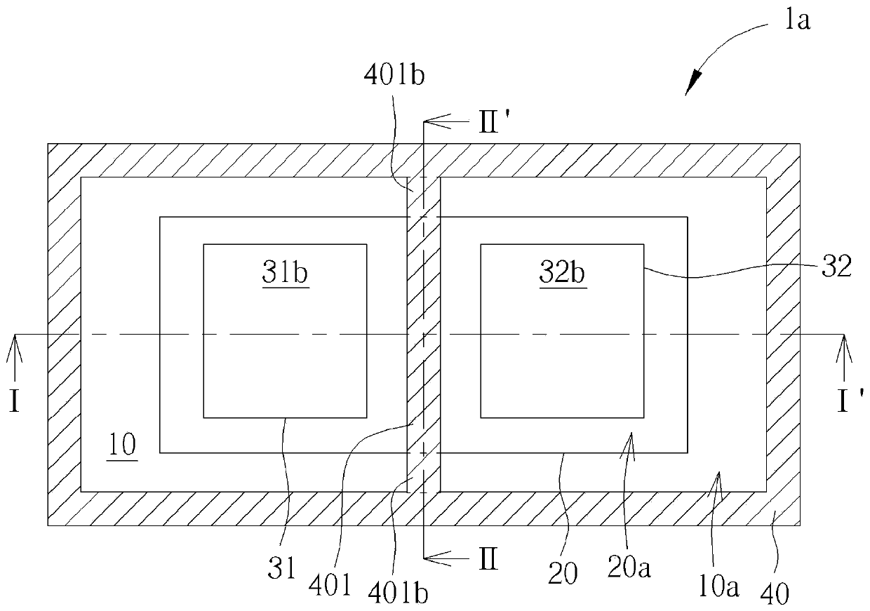
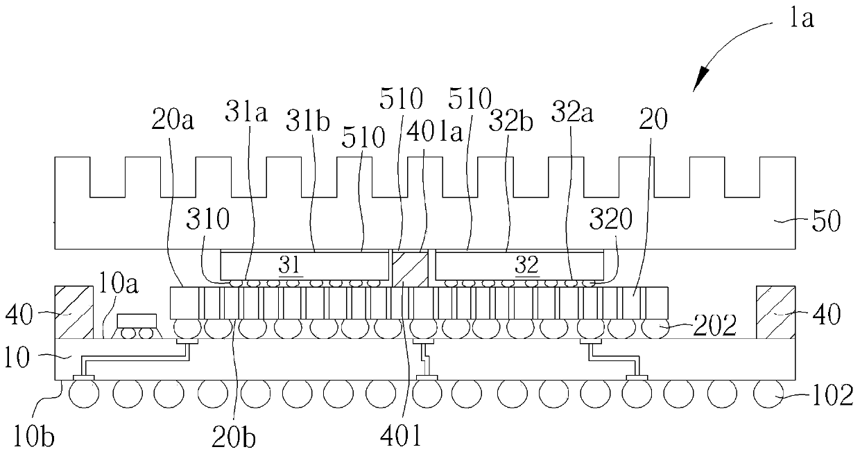
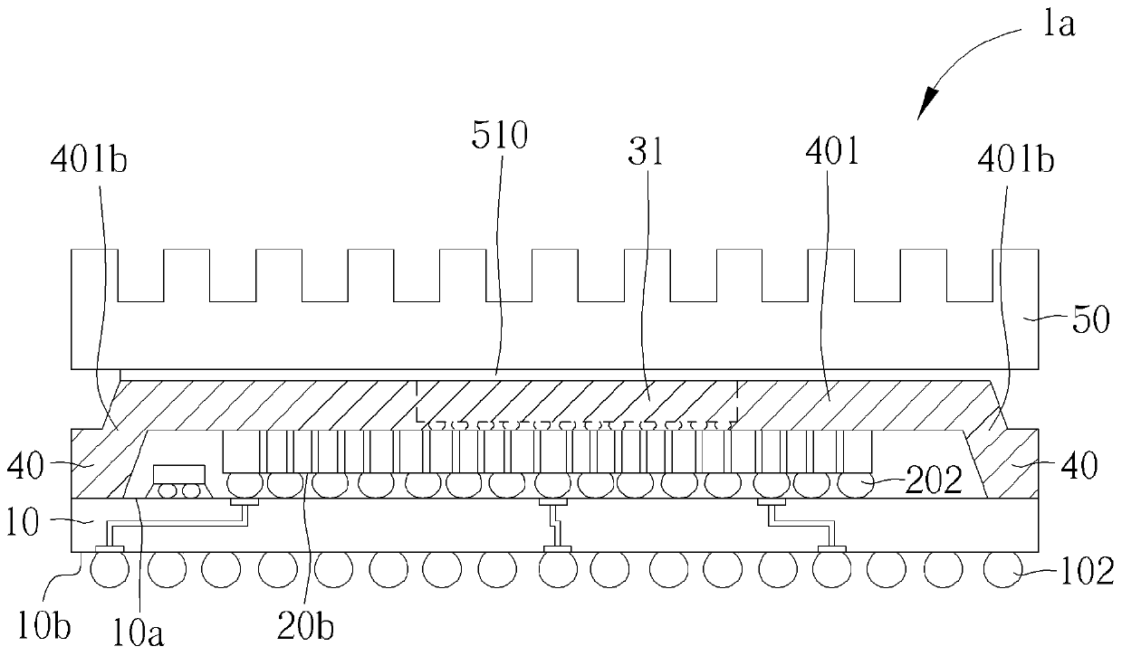
A semiconductor package is disclosed and includes a package substrate having a top surface and a bottom surface, an interposer mounted on the top surface of the package substrate, first semiconductorgrains and second semiconductor grains mounted on the interposer in a side-by-side manner, and a stiffener ring secured to the top surface of the package substrate. The stiffener ring encircles the first semiconductor grains and the second semiconductor grains. The stiffener ring comprises a reinforcement rib striding across the interposer. Through this way, the semiconductor grains are reinforcedwith the stiffener ring and the reinforcement rib, and therefore, coverage and sealing of the semiconductor grains are reduced, heat generated by the semiconductor grains is not blocked by other blocking objects so that heat dissipation of a semiconductor package is not influenced, and the heat dissipation speed and the heat dissipation capability of the semiconductor package are improved. Moreover, the mechanical strength of the semiconductor package can be improved by the stiffener ring and the reinforcement rib, and the warpage of the semiconductor package can be reduced.

Description

technical field [0001] The invention relates to the technical field of semiconductors, in particular to a semiconductor package. Background technique [0002] During operation of an integrated circuit (IC, integrated circuit), the IC chip generates heat, thereby heating the entire electronic device package including the chip. This heat must be dissipated because the performance of the IC chip degrades with increasing temperature, and because high thermal stresses reduce the structural integrity of the electronics package. [0003] Typically, electronic device packages use metal lids to dissipate heat. Heat from the chip is transferred to the metal lid through the chip / lid interface. The heat is then transferred from the metal cover to the surrounding air by convection, or to a heat sink mounted on the metal cover. As die power consumption, die size, and thermal density increase with each new generation of microprocessors, heat dissipation becomes a challenge. Contents o...

Claims


Application Information

Patent Timeline
Patent Type & Authority Applications(China)
IPC IPC(8): H01L25/18H01L23/31H01L23/367H01L23/488H01L23/482
CPCH01L25/18H01L23/3672H01L24/02H01L24/14H01L23/3107H01L2224/1411H01L2224/02333H01L2224/02381H01L23/16H01L23/36H01L23/3675H01L23/49816H01L23/5384H01L23/5385H01L23/562H01L25/0655H01L2224/12105H01L2224/16227H01L2224/73253H01L2924/1433H01L2924/1434H01L2924/1436H01L2924/15192H01L2924/15311H01L2924/18161H01L2924/18162H01L2924/3511
Inventor 潘麒文彭逸轩郭圣良林仪柔陈泰宇
Owner MEDIATEK INC
Learn More