Probe card, preparation method and chip testing method

A probe card and probe technology, used in semiconductor/solid-state device testing/measurement, electrical components, electrical solid-state devices, etc., can solve the problem of electrode pitch reduction, probe alignment difficulties, and difficulty in ensuring accuracy problems, to ensure effective contact, achieve batch testing, and ensure the effect of testing efficiency

Pending Publication Date: 2019-07-23
CHENGDU VISTAR OPTEOLECTRONICS CO LTD
View PDF5 Cites 2 Cited by
  • Summary
  • Abstract
  • Description
  • Claims
  • Application Information

AI Technical Summary

Problems solved by technology

[0003] However, with the increase in the number of electrodes in semiconductor chips and further miniaturization, the pitch between electrodes continues to decrease. Especially for Micro-LED chips, the electrodes have small size, complex surface structure, and ups and downs. Traditional probes use It is difficult to ensure the accuracy of mechanical movement in contact with the chip electrodes, which makes it difficult to align the probes during the test, thus affecting the test efficiency

Method used


Image

  • Probe card, preparation method and chip testing method
  • Probe card, preparation method and chip testing method
  • Probe card, preparation method and chip testing method

Examples


Embodiment Construction

[0044] In order to make the purpose, technical solutions and advantages of the present invention clearer, the technical solutions in the embodiments of the present invention will be clearly and completely described below in conjunction with the embodiments of the present invention. Obviously, the described embodiments are part of the implementation of the present invention. example, not all examples. Based on the embodiments of the present invention, all other embodiments obtained by persons of ordinary skill in the art without making creative efforts belong to the protection scope of the present invention. In the case of no conflict, the following embodiments and features in the embodiments can be combined with each other.

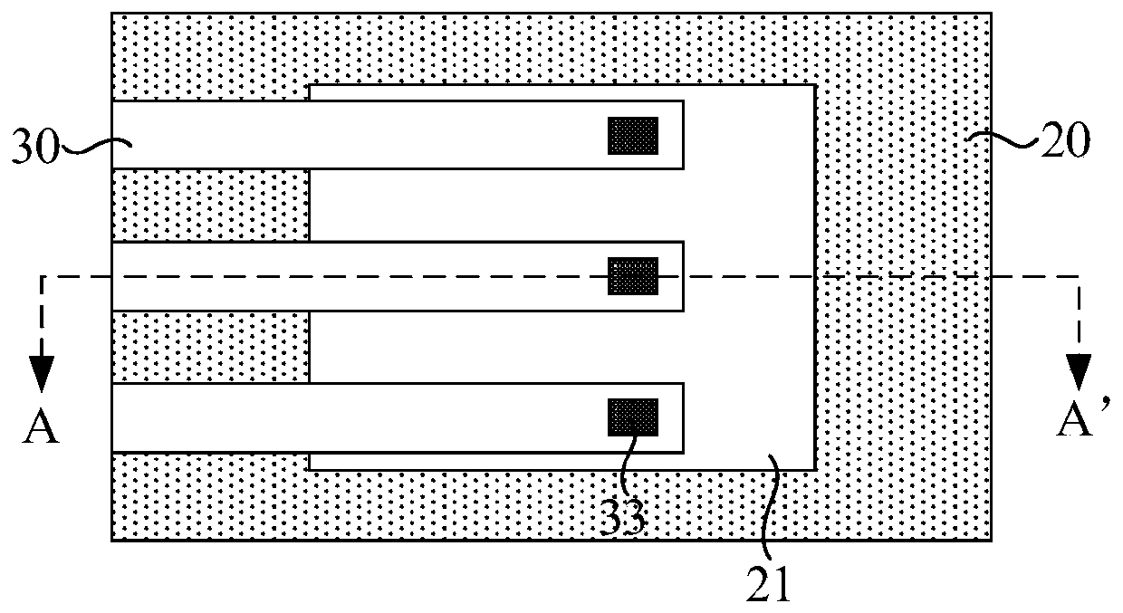
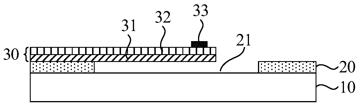
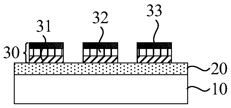
[0045] As mentioned in the background, the test accuracy of the probe card in the prior art cannot meet the test of the existing miniaturized chip. As the chip size becomes smaller, the surface structure of the chip becomes more complex, and it is easy t...


PUM


Abstract

The embodiment of the invention discloses a probe card, a preparation method and a chip testing method. The probe card comprises a substrate and a patterned substrate layer located on one side of thesubstrate. The patterned substrate layer comprises at least one vacant groove and at least one cantilever probe located on the side, away from the substrate, of the patterned substrate layer. The cantilever probe extends to the vacant groove and is suspended on the vacant groove. The cantilever probe comprises a first thermal deformation layer, a second thermal deformation layer and a conductive contact. The first thermal deformation layer is located between the patterned substrate layer and the second thermal deformation layer, the thermal expansion coefficient of the first thermal deformation layer is larger than that of the second thermal deformation layer, the conductive contact is arranged at the end, suspended in the vacant groove, of the cantilever probe, the first thermal deformation layer and/or the second thermal deformation layer are/is a conductive layer, and the conductive layer is electrically connected with the conductive contact. The cantilever probe card solves the problems that an existing probe card is insufficient in butt joint precision and prone to poor contact, automatic contact of the probe is achieved, and effective contact between the cantilever probe anda chip to be detected can be guaranteed.

Description

technical field [0001] The embodiments of the present invention relate to the technical field of semiconductor manufacturing, and in particular to a probe card, a preparation method and a chip testing method. Background technique [0002] Various tests are required at various stages of semiconductor device manufacturing. For example, in order to test the electrical characteristics of the semiconductor device before packaging the semiconductor device, a test instrument can be used as an interface connected to the semiconductor device through a probe card that includes fine probes. Specifically, the probes of the probe card can be connected to the semiconductor device. The upper electrode contacts are electrically connected so that an electrical signal can be transmitted from the tester to the semiconductor device, and a signal output from the semiconductor device in response to the transmitted electrical signal is detected and analyzed to determine whether the semiconductor d...

Claims


Application Information

Patent Timeline
Patent Type & Authority Applications(China)
IPC IPC(8): H01L21/66H01L27/15
CPCH01L22/14H01L27/156
Inventor 邢汝博
Owner CHENGDU VISTAR OPTEOLECTRONICS CO LTD
Why Eureka
Try Eureka