Supercharge Your Innovation With Domain-Expert AI Agents!

Input interface circuit for chip enable control

A technology for inputting interface circuits and chips, applied in logic circuits with logic functions, logic circuit coupling/interface using field effect transistors, logic circuits, etc. break and other problems to ensure the effect of normal work

Active Publication Date: 2019-07-30
UNIV OF ELECTRONICS SCI & TECH OF CHINA
View PDF4 Cites 4 Cited by
  • Summary
  • Abstract
  • Description
  • Claims
  • Application Information

AI Technical Summary

Problems solved by technology

At the moment when the chip is turned on and off, due to environmental interference, the enable control signal is usually subject to noise interference and pulse interference, causing the chip to be triggered to turn on or off by mistake, resulting in the collapse of the system where the chip is located. Therefore, the designed chip enable control The input interface circuit is particularly important

Method used


Image

  • Input interface circuit for chip enable control
  • Input interface circuit for chip enable control
  • Input interface circuit for chip enable control

Examples


Embodiment Construction

[0028] The technical solution of the present invention will be described in detail below in conjunction with the accompanying drawings and specific embodiments.

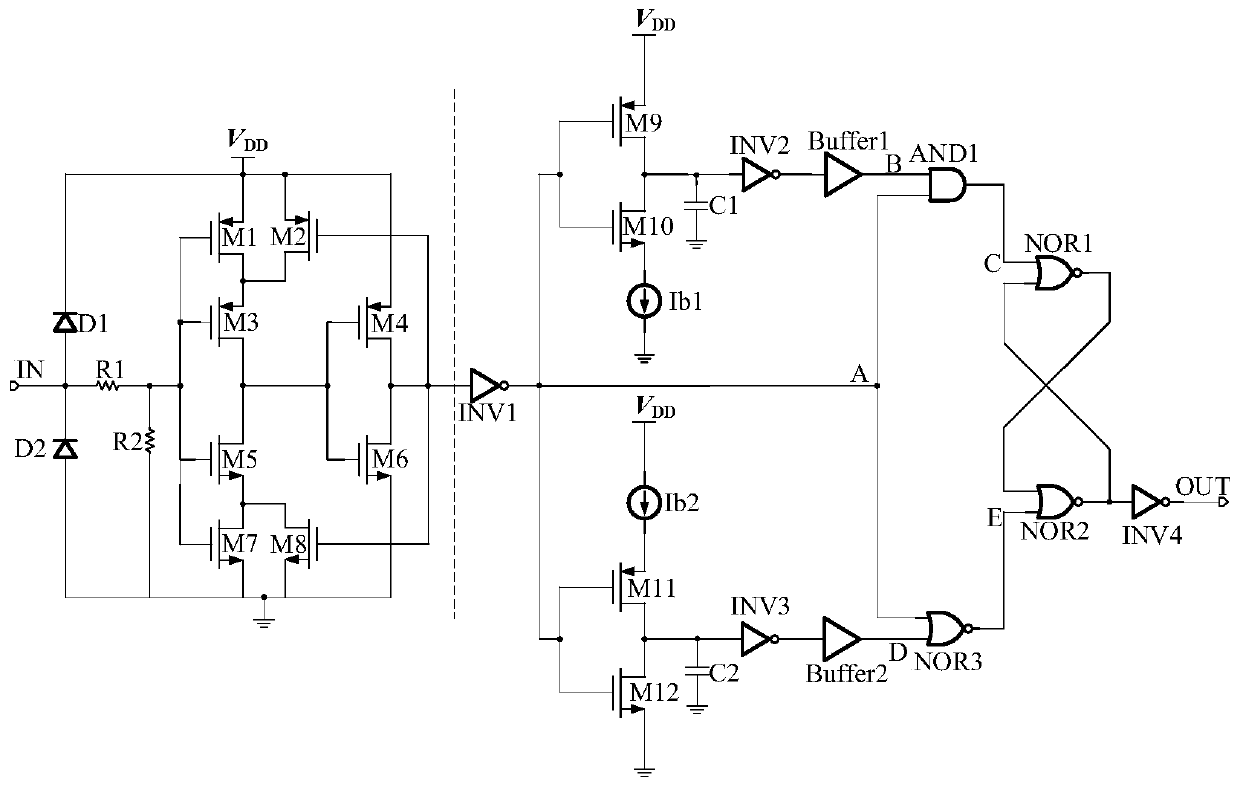
[0029] An input interface circuit for chip enable control proposed by the present invention includes a hysteresis circuit and a pulse filter circuit, wherein the hysteresis circuit is used to filter noise signals in the input signal IN of the input interface circuit, and its input terminal is connected to the input interface The input signal IN of the circuit, its output terminal is connected to the input terminal of the pulse filter circuit, such as figure 1 The diagram shows an implementation form of the hysteresis circuit, including the third NMOS transistor M5, the fourth NMOS transistor M6, the fifth NMOS transistor M7, the sixth NMOS transistor M8, the third PMOS transistor M1, the fourth PMOS transistor M2, The fifth PMOS transistor M3, the sixth PMOS transistor M4, the first resistor R1, the second resistor R...


PUM


Abstract

An input interface circuit for chip enable control comprises a hysteresis circuit and a pulse filter circuit. The hysteresis circuit filters noise signals in a hysteresis window through a hysteresis comparator of an up-down symmetrical structure. The pulse filtering circuit preprocesses short pulse interference signals through a pulse filtering preprocessing circuit composed of a first PMOS transistor, a first NMOS transistor, a first current source, a first capacitor, a second PMOS transistor, a second NMOS transistor, a second current source and a second capacitor. The obtained signal is transmitted to a first NOR gate and a second NOR gate or a non-RS trigger. By utilizing the characteristic that the output remains unchanged when the input at the two ends of the non-RS contact pressuredevice is zero at the same time, unnecessary short pulse interference signals are filtered out, and the short pulse interference signals with different pulse widths can be filtered out by adjusting the magnitude of a current source and the magnitude of capacitance. The external enable control signal of the chip can be restored, so that the chip is normally controlled, the chip is prevented from being mistakenly triggered to be turned off or turned on, and the normal work of a system where the chip is located is ensured.

Description

technical field [0001] The invention belongs to the technical field of electronic circuits, and in particular relates to an input interface circuit used for chip enable control. Background technique [0002] In today's information and digital society, electronic information technology is developing rapidly. Due to the uncontrollability and low reliability of traditional circuits, more and more intelligent circuit systems are replacing traditional circuits. As the core of the intelligent circuit system, the chip usually needs to have an enabling control terminal in order to cooperate with the normal operation of the entire circuit system. Enable control, in short, is to turn on or turn off a chip with a certain function according to the needs of the intelligent circuit system. The chip is controlled by an intelligent circuit system, which can improve the reliability of the entire system. At the moment when the chip is turned on and off, due to environmental interference, th...

Claims


Application Information

Patent Timeline
IPC IPC(8): H03K19/003H03K19/0185H03K19/20
CPCH03K19/00315H03K19/00361H03K19/018507H03K19/20
Inventor 李泽宏胡任任洪至超仪梦帅杨尚翰杨耀杰
Owner UNIV OF ELECTRONICS SCI & TECH OF CHINA
Features
  • R&D
  • Intellectual Property
  • Life Sciences
  • Materials
  • Tech Scout
  • Unparalleled Data Quality
  • Higher Quality Content
  • 60% Fewer Hallucinations
Learn More