Multi-layer circuit board machining method

A processing method and multi-layer circuit technology, applied in the direction of multi-layer circuit manufacturing, printed circuit, printed circuit manufacturing, etc., can solve the problems of high processing cost, many repeated processes, and many times of pressing, so as to improve production efficiency and reduce Manufacturing cost, effect of reducing the number of pressing

Inactive Publication Date: 2019-07-30
SHENZHEN SUNWAY COMM
View PDF4 Cites 6 Cited by
  • Summary
  • Abstract
  • Description
  • Claims
  • Application Information

AI Technical Summary

Problems solved by technology

Therefore, the existing multi-layer circuit board processing method has complicated process and many repeated processes (more pressing times), resulting in high processing cost

Method used


Image

  • Multi-layer circuit board machining method
  • Multi-layer circuit board machining method
  • Multi-layer circuit board machining method

Examples


Embodiment 1

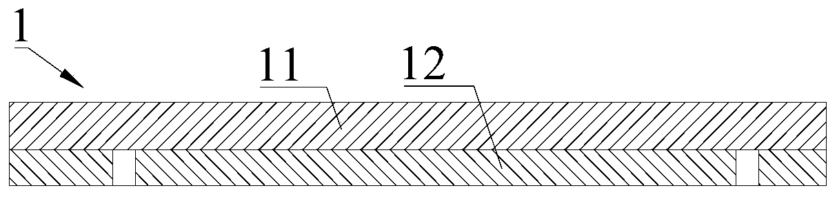
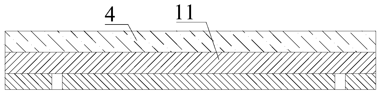
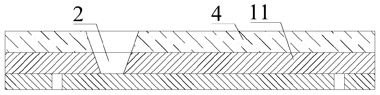
[0039] Please refer to Figure 1 to Figure 6 , Embodiment one of the present invention is: multilayer circuit board processing method, comprises the following steps,

[0040] S1. Make preset circuits for each plate 1 respectively;

[0041] S2. Stack each plate 1 in a preset order to obtain a stack of plates;

[0042] S3. Laminating the sheet stack at one time to obtain a multilayer circuit board.

[0043] In step S1 , making the preset circuit includes opening a via hole 2 , and step S11 before step S2 includes printing conductive paste 3 into the via hole 2 . The conductive paste 3 is used to connect two adjacent boards 1 . The via hole 2 can be a through hole or a blind hole. It should be understood that there may be individual boards 1 that do not need to be connected to other boards 1 , so the conduction holes 2 do not need to be opened on the individual boards 1 . The conductive paste 3 may be copper paste or the like.

[0044] Preferably, in step S1, when opening t...


PUM


Abstract

The invention discloses a multi-layer circuit board machining method; the multi-layer circuit board machining method comprises the following steps of S1, carrying out preset circuit manufacturing on each board separately; S2, stacking the boards in a preset sequence so as to obtain a board pile; and S3, pressing the board pile at a time to obtain a multilayer circuit board. In the manufacturing process of the multi-layer circuit board, only one-time lamination is needed, so that the laminating frequency is greatly reduced, the production efficiency is favorably improved, the manufacturing costof the multi-layer circuit board is reduced; and the size precision of the multi-layer circuit board formed by one-time lamination is higher.

Description

technical field [0001] The invention relates to the technical field of circuit board processing, in particular to a multilayer circuit board processing method. Background technique [0002] Multilayer circuit board is the product of the development of electronic technology in the direction of high speed, multi-function, large capacity and small volume. With the continuous development of electronic technology, especially the extensive and in-depth application of large-scale and ultra-large-scale integrated circuits, multilayer circuit boards are rapidly developing towards high-density, high-precision, and high-level digitization. [0003] Multilayer circuit boards include multiple laminated boards. In the prior art, when making multilayer circuit boards, the inner layer circuits on the inner layer boards are first made, and then pressed with the outer layer boards, and then exposed with high-precision exposure equipment. After completing the production of the outer circuit, ...

Claims


Application Information

Patent Timeline
Patent Type & Authority Applications(China)
IPC IPC(8): H05K3/46
CPCH05K3/4611
Inventor 谈兴李绪东虞成城余辉张辉
Owner SHENZHEN SUNWAY COMM
Why Eureka
Try Eureka