Manufacturing method of semiconductor device

A manufacturing method and semiconductor technology, applied in the fields of semiconductor/solid-state device manufacturing, semiconductor devices, electric solid-state devices, etc., can solve the problems of plasma difficulties, rising process costs, complex process flow, etc., to change the charge distribution, improve the plasma Damage, the effect of optimizing the process

Inactive Publication Date: 2019-08-06
WUHAN XINXIN SEMICON MFG CO LTD
View PDF7 Cites 0 Cited by
  • Summary
  • Abstract
  • Description
  • Claims
  • Application Information

AI Technical Summary

Problems solved by technology

However, as the size of flash memory devices continues to decrease, it becomes more and more difficult to solve the problem of PID by reducing the energy of the plasma, the process becomes more and more complicated, and the process cost rises sharply

Method used


Image

  • Manufacturing method of semiconductor device

Examples


Embodiment Construction

[0026] The following will clearly and completely describe the technical solutions in the embodiments of the present invention with reference to the accompanying drawings in the embodiments of the present invention. Obviously, the described embodiments are only some, not all, embodiments of the present invention. Based on the embodiments of the present invention, all other embodiments obtained by persons of ordinary skill in the art without creative efforts fall within the protection scope of the present invention.

[0027] It should be noted that, in the case of no conflict, the embodiments of the present invention and the features in the embodiments can be combined with each other.

[0028] The present invention will be further described below in conjunction with the accompanying drawings and specific embodiments, but not as a limitation of the present invention.

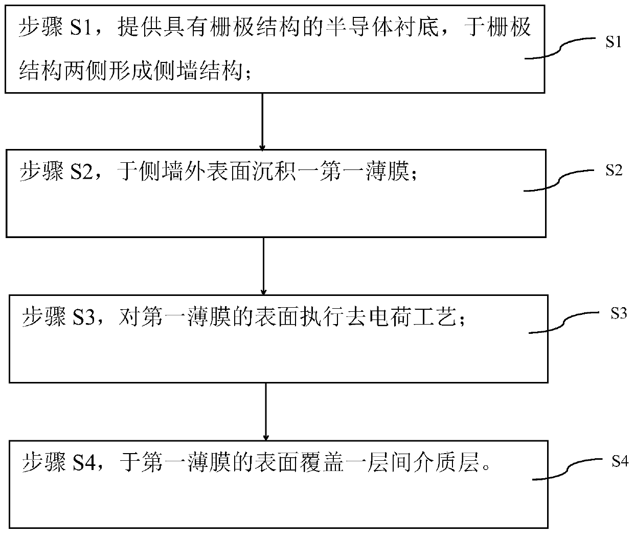
[0029] The present invention includes a method of manufacturing a semiconductor device, such as figure 1 shown,...


PUM


Abstract

The invention relates to the technical field of semiconductor manufacturing, and particularly relates to a manufacturing method of a semiconductor device. The manufacturing method comprises the stepsof S1, providing a semiconductor substrate with a gate structure, and forming a side wall structure on both sides of the gate structure; S2, depositing a first thin film on the outer surface of each side wall; S3, performing a charge removing process on the surface of the first thin film; and S4, covering the surface of the first thin film with an interlayer dielectric layer. The technical schemeof the invention has the beneficial effects that the charge distribution on the wafer surface is changed through optimizing the chemical deposition process, and the plasma damage can be improved.

Description

technical field [0001] The invention relates to the technical field of semiconductor manufacturing, in particular to a method for manufacturing a semiconductor device. Background technique [0002] In the manufacturing process of flash memory devices (Flash), the problem of PID (Plasma Induced Damage, plasma damage) is a common reliability problem. In the process of high-density plasma, due to the unbalanced The electric field will cause irreversible damage to the gate oxide, and PID is crucial to the reliability of the product. [0003] The existing solution mainly solves the PID problem by reducing the energy of plasma (plasma) through multi-channel processes. However, as the size of flash memory devices continues to decrease, it becomes more and more difficult to solve the PID problem by reducing the energy of the plasma, the process flow becomes more and more complicated, and the process cost rises sharply. Therefore, there is an urgent need for a manufacturing method ...

Claims


Application Information

Patent Timeline
Patent Type & Authority Applications(China)
IPC IPC(8): H01L21/285H01L21/3105H01L27/11521H01L27/11568C23C16/40
CPCH01L21/285H01L21/3105C23C16/402H10B43/30H10B41/30
Inventor 王辉龙俊舟侯多源
Owner WUHAN XINXIN SEMICON MFG CO LTD
Why Eureka
Try Eureka