A kind of avalanche photodiode diffusion structure, preparation method and diode device
A diffusion structure, avalanche photoelectric technology, applied in the field of photodetectors, can solve the problems of low device reliability, high device cost, low device yield, etc., and achieve the effects of suppressing edge breakdown, uniform breakdown voltage, and optimizing edge curvature
- Summary
- Abstract
- Description
- Claims
- Application Information
AI Technical Summary
Problems solved by technology
Method used
Image
Examples
Embodiment 1
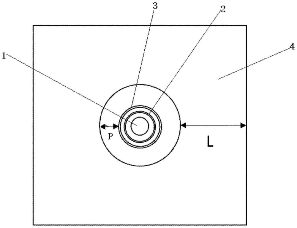
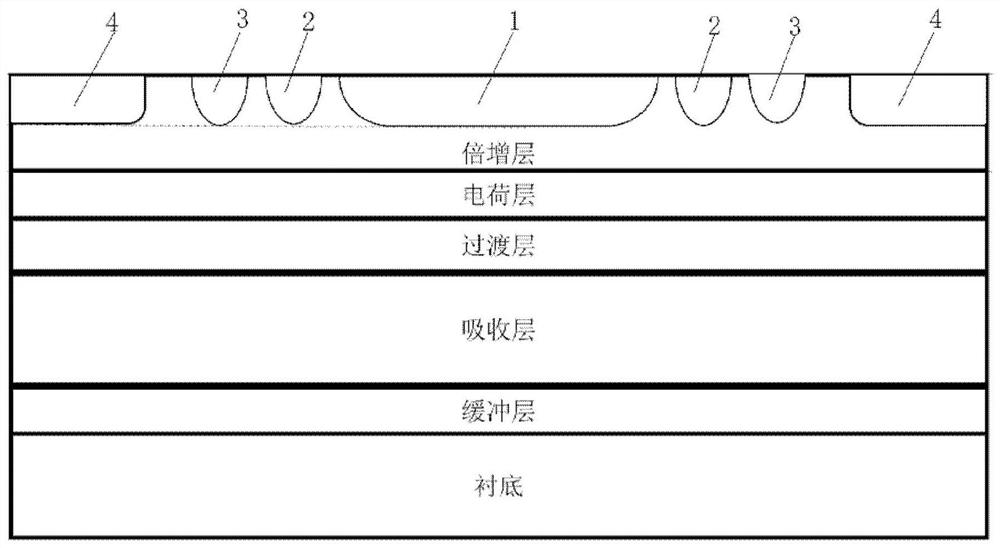
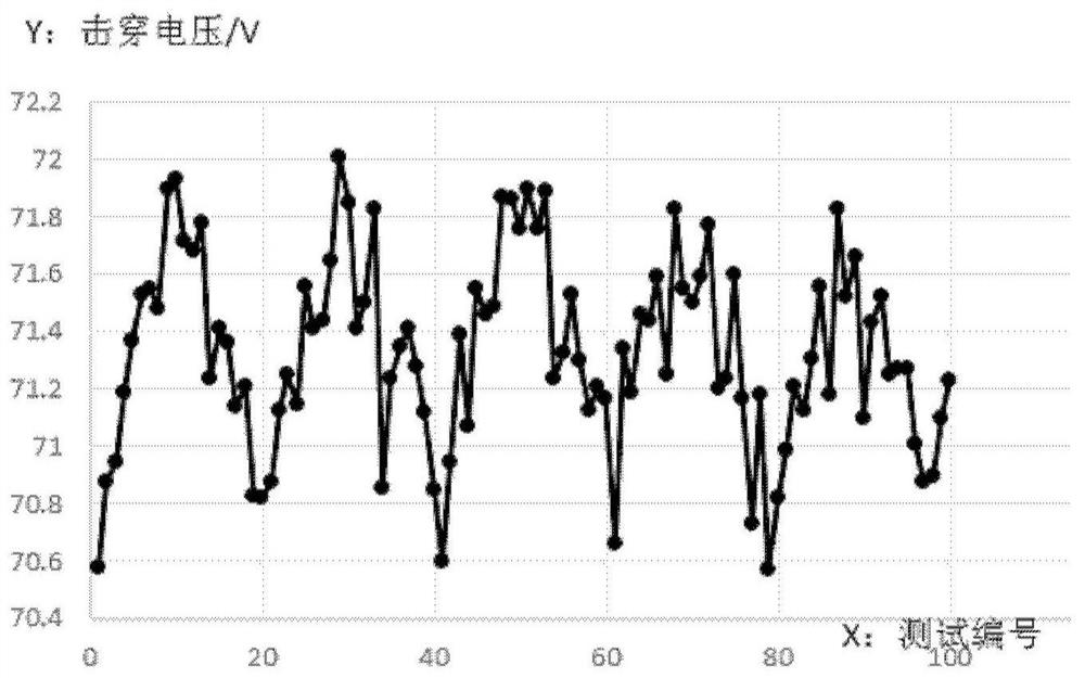
[0037] In this embodiment, 100 samples selected from the same wafer are selected to test the breakdown voltage, and the 100 samples all have a diffusion trench region, a first guard ring, and a second guard ring;
[0038] The test results are as image 3 As shown, the range of the breakdown voltage of 100 samples selected from the same wafer is 1.44V, and the percentage of the corresponding deviation is slightly less than 2%. And the uniformity of its breakdown voltage is excellent (the average value is about 71V).
Embodiment 2
[0040] In this embodiment, 100 samples selected from the same wafer are selected to test the breakdown voltage, and the 100 samples all have the first guard ring and the second guard ring, but do not have the diffusion trench region;
[0041] The test results are as Figure 4 As shown, although there is a first guard ring and a second guard ring to suppress the edge breakdown and ensure a larger breakdown voltage (average value is about 72V), due to the non-diffusion trench area, the diffusion depth of each active area is different, and its The uniformity of the breakdown voltage is extremely poor, and the extreme difference of the breakdown voltage of 100 samples selected from the same wafer is 11.57V, and the corresponding deviation percentage is about 16%.
Embodiment 3
[0043] In this embodiment, 100 samples selected from the same wafer are selected to test the breakdown voltage, and the 100 samples all have diffusion trench regions, but do not have the first guard ring and the second guard ring;
[0044] The test results are as Figure 5 As shown, although there is a diffusion trench area to maintain the uniformity of diffusion in the active area, the edge breakdown of the device cannot be suppressed because there is no guard ring structure, and the edge breakdown of different devices is different, resulting in premature breakdown of some devices. As a result, the breakdown voltage is relatively small (average value is about 66V), and the edge breakdown conditions of different samples are different, resulting in poor uniformity of the breakdown voltage. 100 samples were selected from the same wafer to test the extreme breakdown voltage. The difference is: 8.6V, corresponding to a percentage of deviation of about 13%.
[0045] Therefore, the...
PUM
| Property | Measurement | Unit |
|---|---|---|
| diameter | aaaaa | aaaaa |
| width | aaaaa | aaaaa |
| width | aaaaa | aaaaa |
Abstract
Description
Claims
Application Information


