

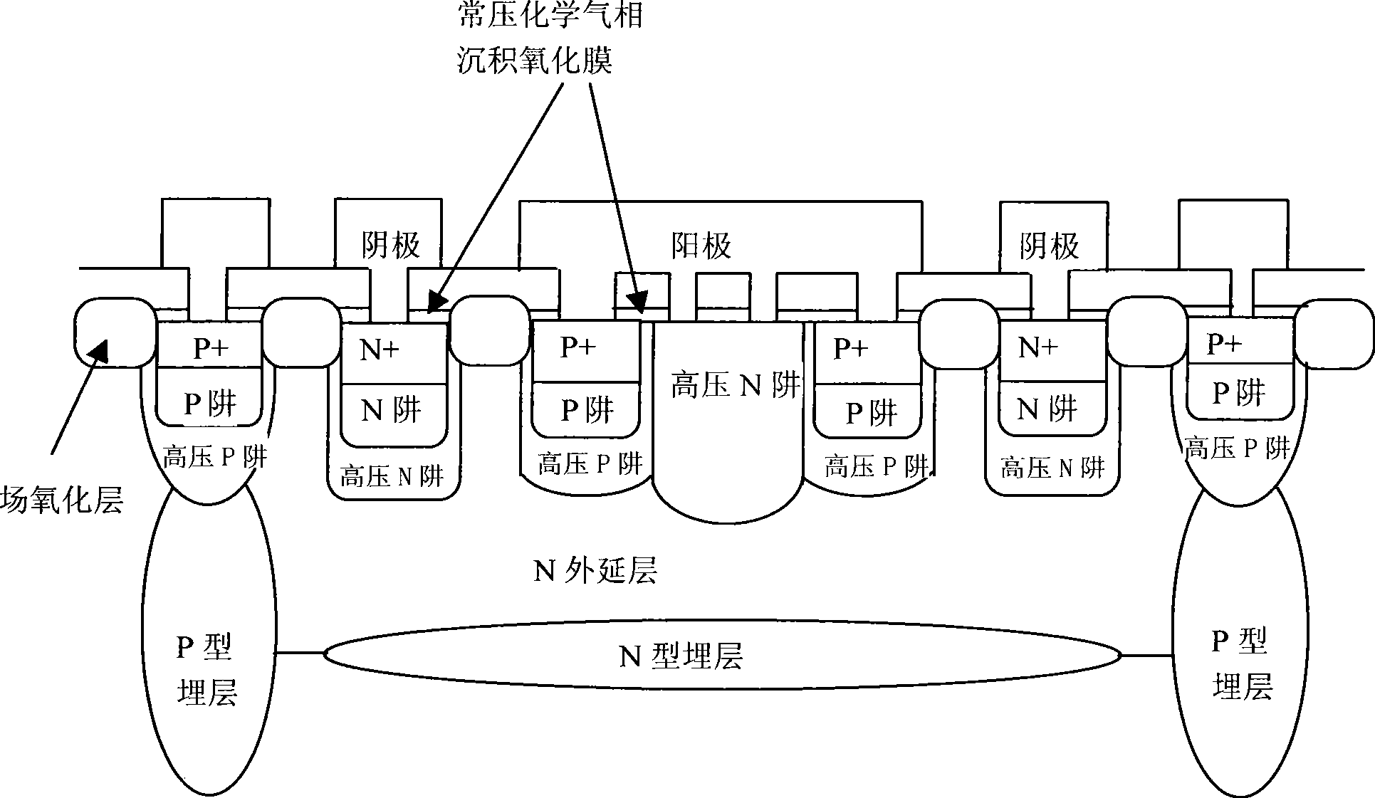
Manufacturing method for integrated schottky diode
A technology of Schottky diode and manufacturing method, applied in semiconductor/solid-state device manufacturing, electrical components, circuits, etc., can solve the problems of low breakdown voltage of integrated Schottky diode, uneven guard ring, poor uniformity, etc. The protection ring is uniform, the interface layer is easy to repair, and the effect of high breakdown voltage
- Summary
- Abstract
- Description
- Claims
- Application Information
AI Technical Summary
Problems solved by technology
Method used
Image

Examples
Embodiment Construction
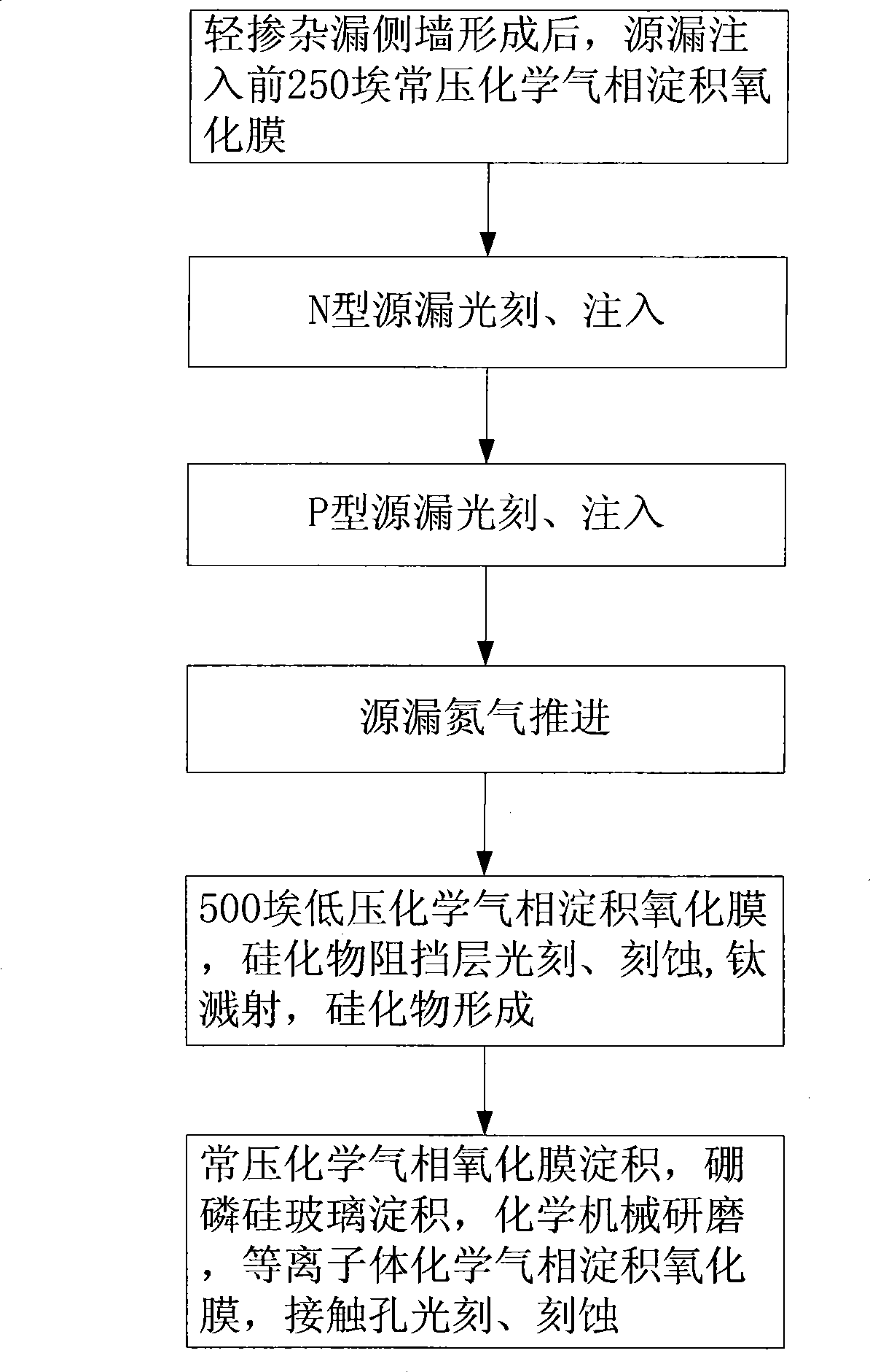
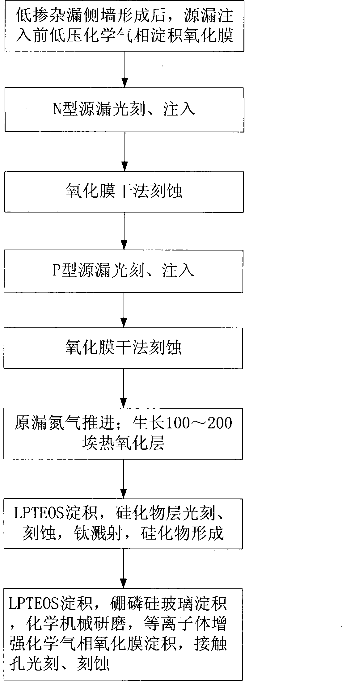
[0034] An embodiment of the integrated Schottky diode manufacturing method of the present invention is as follows image 3 shown, including the following steps:
[0035] (1) Low-pressure chemical vapor deposition oxide film (LPTEOS) after the low-doped drain sidewall (LDD) is formed;
[0036] (2) N-type source-drain (NSD) lithography and implantation;
[0037] (3) LPTEOS dry etching;
[0038] (4) P-type source-drain (PSD) lithography and implantation;
[0039] (5) LPTEOS dry etching;
[0040] (6) Source-drain (SD) nitrogen propulsion; growth of 100-200 angstrom thermal oxide layer;
[0041] (7) 500 Angstrom LPTEOS deposition, silicide layer (SB) photolithography, etching, titanium sputtering, silicide (silicide) formation;
[0042] (8) LPTEOS deposition, borophosphosilicate glass deposition (BPSG), chemical mechanical polishing (CMP), plasma enhanced chemical phase deposition oxide film (PETEOS) deposition, contact hole (CT) lithography and etching.
[0043] The differen...
PUM
 Abstract
Description
Claims
Application Information