Method for manufacturing semiconductor devices

A manufacturing method, semiconductor technology, applied in semiconductor/solid-state device manufacturing, semiconductor devices, electric solid-state devices, etc., can solve problems such as separation, and achieve the effect of improving adhesion, reliability and life

Inactive Publication Date: 2003-02-05
NEC CORP
View PDF1 Cites 0 Cited by
  • Summary
  • Abstract
  • Description
  • Claims
  • Application Information

AI Technical Summary

Problems solved by technology

The same type of problem of separation also exists in these cases

Method used


Image

  • Method for manufacturing semiconductor devices
  • Method for manufacturing semiconductor devices
  • Method for manufacturing semiconductor devices

Examples


Embodiment Construction

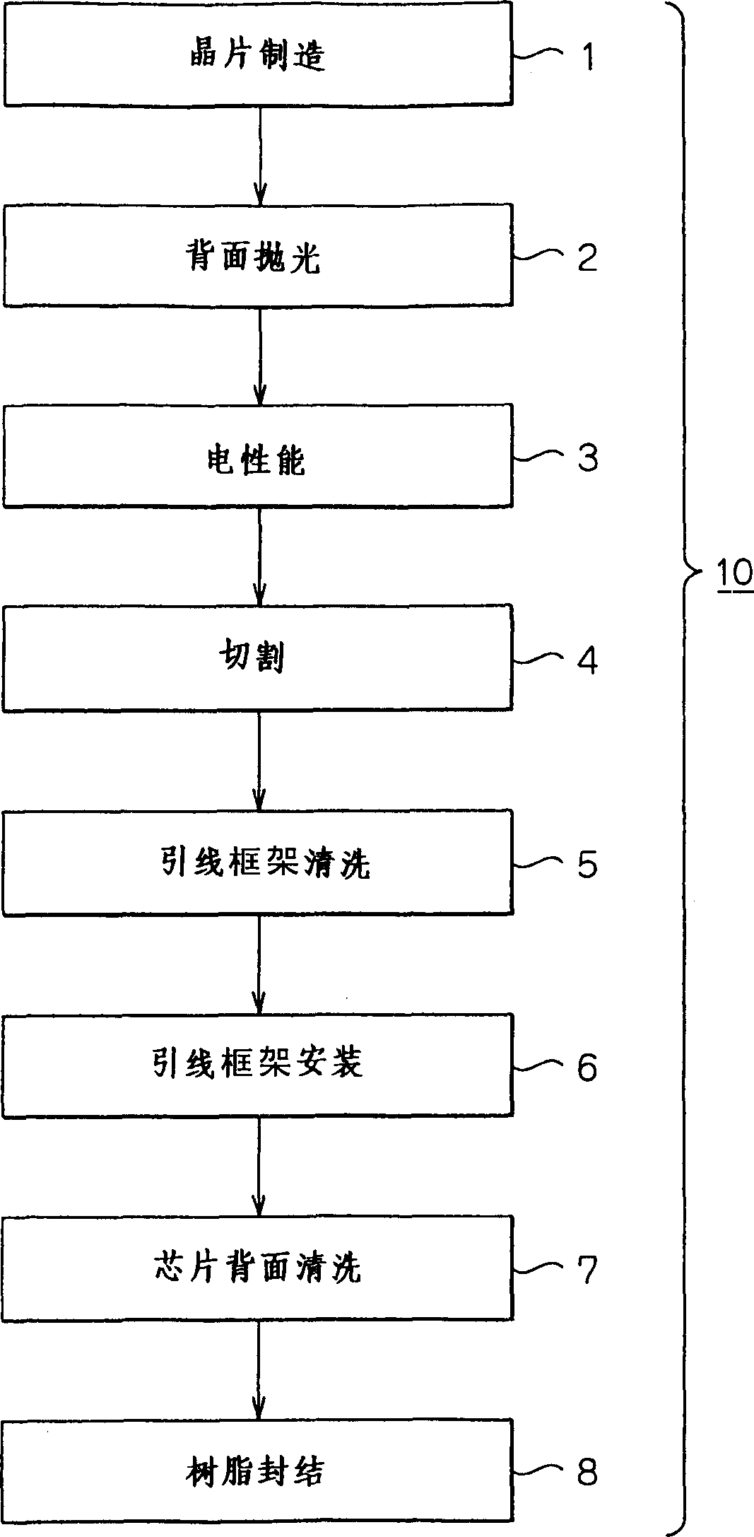
[0037] figure 1 is a flowchart of the manufacturing method 10 of the semiconductor device 11 . The manufacturing method 10 includes the following steps: a wafer manufacturing process 1, a backside polishing process 2, an electrical property measurement process 3, a cutting process 4, a lead frame cleaning process 5, a lead frame mounting process 6, a chip back cleaning process 7, and resin sealing Process 8. Perform the above process in the order shown in the figure.

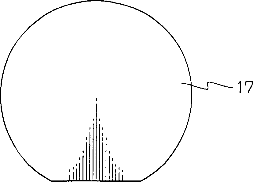
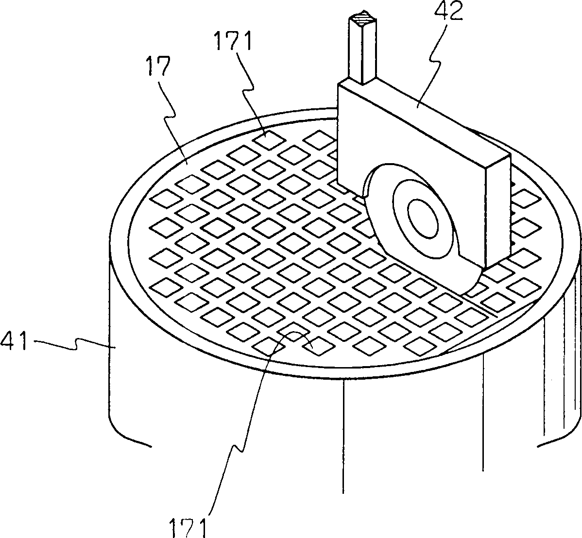
[0038] In the wafer manufacturing process 1, a 0.2-0.3mm thick oxide film (SiO 2 ) covering a flat silicon wafer 17 ( figure 2 ) on the upper surface; and the circuit patterns of the active circuits thereon are exposed and developed. The oxide layer is then etched into the circuit pattern. Thereafter, an infinite number of active circuits 171 are formed on the surface by doping the exposed surface of the wafer 17 (see image 3 ).

[0039] In the backside polishing process 2, the surface (backside) of the...


PUM


Abstract

The invention relates to a manufacturing method of a semiconductor device for preventing separation of resin and a semiconductor chip. The manufacturing method comprises cutting a wafer having an active circuit formed on a surface of the wafer and forming the semiconductor chip; mounting a group of lead terminals on the semiconductor chip; and washing the surface of the semiconductor chip at a reverse face of the active circuit. And then the semiconductor chip is sealed by sealing marerial. Thereby the separation of the resin and the semiconductor chip is prevented.

Description

technical field [0001] The invention relates to a method for manufacturing a semiconductor device. Background technique [0002] A semiconductor device was manufactured by the method described below. [0003] Active circuits with multiple semiconductor chips are formed on a wafer. Polish the wafer surface opposite the active circuitry. Perform measurements on the electrical properties of active circuits. The semiconductor chip is attached to the lead frame with an adhesive. The outgoing terminal of the active circuit is connected with the lead wire of the lead frame. Semiconductor chips are buried in resin. Let the resin harden completely. Lead terminals outside the plating resin. [0004] Cut off and trim the excess of the leads, then bend the leads. Finally, the electrical performance of the semiconductor product is tested. [0005] In the above process, the semiconductor chip is fixed in the resin without cleaning as it is separated from the wafer. In this case,...

Claims


Application Information

Patent Timeline
IPC IPC(8): H01L21/304H01L21/48H01L21/50
CPCH01L2224/73215H01L21/00
Inventor 滝泽朋子
Owner NEC CORP
Why Eureka
Try Eureka