OLED package structure, OLED package method and display device
A packaging structure and device technology, applied in the direction of semiconductor devices, electrical solid devices, organic semiconductor devices, etc., can solve problems affecting production yield, device dark lines, affecting electrical properties, etc., to improve yield and competitiveness, box thickness Uniform, crush-resistant effect
- Summary
- Abstract
- Description
- Claims
- Application Information
AI Technical Summary
Problems solved by technology
Method used
Image

Examples
Embodiment 1
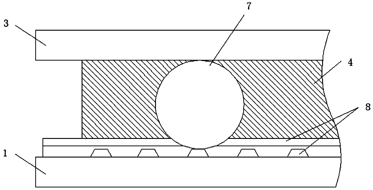
[0032] Such as Figure 2-Figure 4 As shown, Embodiment 1 of the present invention proposes an OLED packaging structure for packaging the OLED device 2 on the display substrate 1. The OLED packaging structure includes:
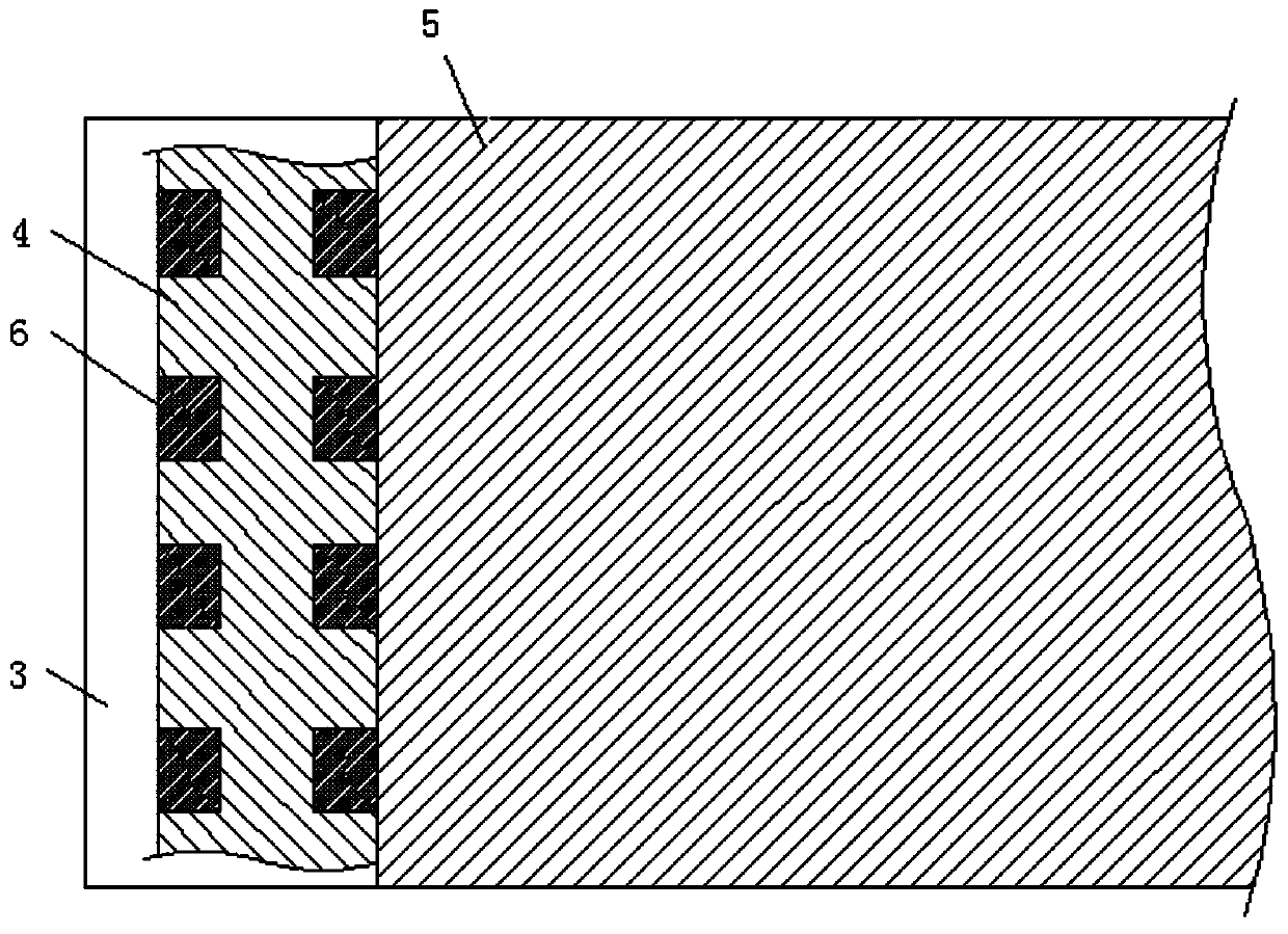
[0033] Encapsulation cover plate 3, the first surface edge of the package cover plate 3 opposite to the display substrate 1 is surrounded by a sealant layer 4, and the area surrounded by the sealant layer 4 is filled with a filler layer 5;
[0034] Wherein, a plurality of support blocks 6 with preset flexibility are distributed in the region corresponding to the sealant layer 4 , and the support blocks are used to fix the thickness of the box between the packaging cover plate and the display substrate.
[0035] Specifically, the existing OLED encapsulation methods mostly use the encapsulation cover plate 3 for encapsulation, the encapsulation cover plate is arranged on the upper side of the display substrate 1, the OLED device is arranged on the surface of the ...
Embodiment 2
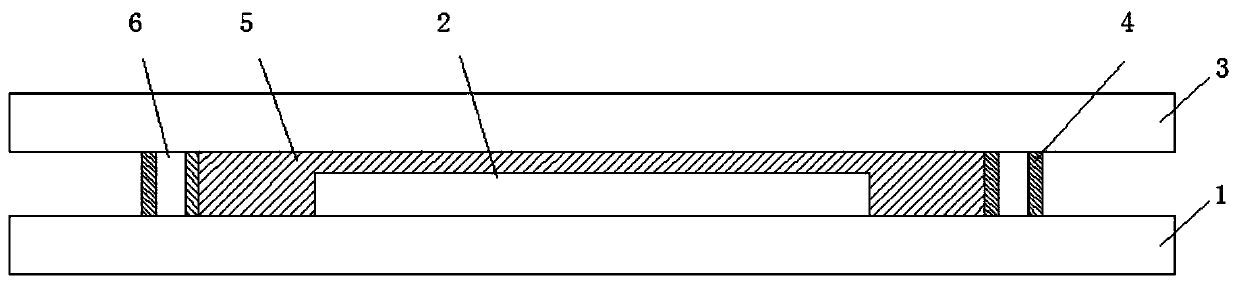
[0044] Such as Figure 5 As shown, Embodiment 2 of the present invention proposes an OLED encapsulation method, the OLED encapsulation method comprising:
[0045] S1: making the support block 6, and arranging the support block 6 on the edge of the first surface of the packaging cover plate 3;
[0046] S2: Coating a sealant layer 4 around the edge of the first surface of the packaging cover plate 3;
[0047] S3: coating the filling glue layer 5 in the area surrounded by the sealing glue layer 4;
[0048] S4: Pressing the packaging cover plate 3 and the display substrate 2, and curing the sealing glue layer 4 and the filling glue layer 5.
[0049] Embodiment 2 of the present invention proposes an OLED encapsulation method. By setting a plurality of support blocks at the edge of the encapsulation cover plate corresponding to the encapsulation adhesive layer, the box thickness can be fixed during the process of laminating the encapsulation cover plate and the display substrate. ...
Embodiment 3
[0052] Embodiment 3 of the present invention provides a display device, which includes: the above-mentioned OLED encapsulation structure.
[0053] Embodiment 3 of the present invention proposes a display device. By arranging a plurality of support blocks at the edge of the packaging cover corresponding to the packaging adhesive layer of the packaging structure, it can act as a fixing box during the process of pressing the packaging cover and the display substrate. thickness, to ensure uniform thickness of the box, especially for large-sized display devices, the effect is more obvious. Due to the preset flexibility of the support block, excessive pressure will not be exerted on the display substrate during the pressing process of the package cover plate and the display substrate, which can prevent the crushing of the exposed wires or affect the electrical properties after contacting the electrodes. It can improve the display image quality of the display device, and can improve ...
PUM
 Abstract
Description
Claims
Application Information
 - R&D
- Intellectual Property
- Life Sciences
- Materials
- Tech Scout
- Unparalleled Data Quality
- Higher Quality Content
- 60% Fewer Hallucinations
Browse by: Latest US Patents, China's latest patents, Technical Efficacy Thesaurus, Application Domain, Technology Topic, Popular Technical Reports.
© 2025 PatSnap. All rights reserved.Legal|Privacy policy|Modern Slavery Act Transparency Statement|Sitemap|About US| Contact US: help@patsnap.com