Display substrate, preparation method thereof, and display device
A technology for display substrates and display areas, which is applied in semiconductor/solid-state device manufacturing, electrical components, electric solid-state devices, etc. It can solve the problems of high production cost, difficult design, and difficult process realization, so as to ensure effectiveness and reliability , to achieve the effect of full screen and borderless screen, good application prospects
- Summary
- Abstract
- Description
- Claims
- Application Information
AI Technical Summary
Problems solved by technology
Method used
Image

Examples
no. 1 example
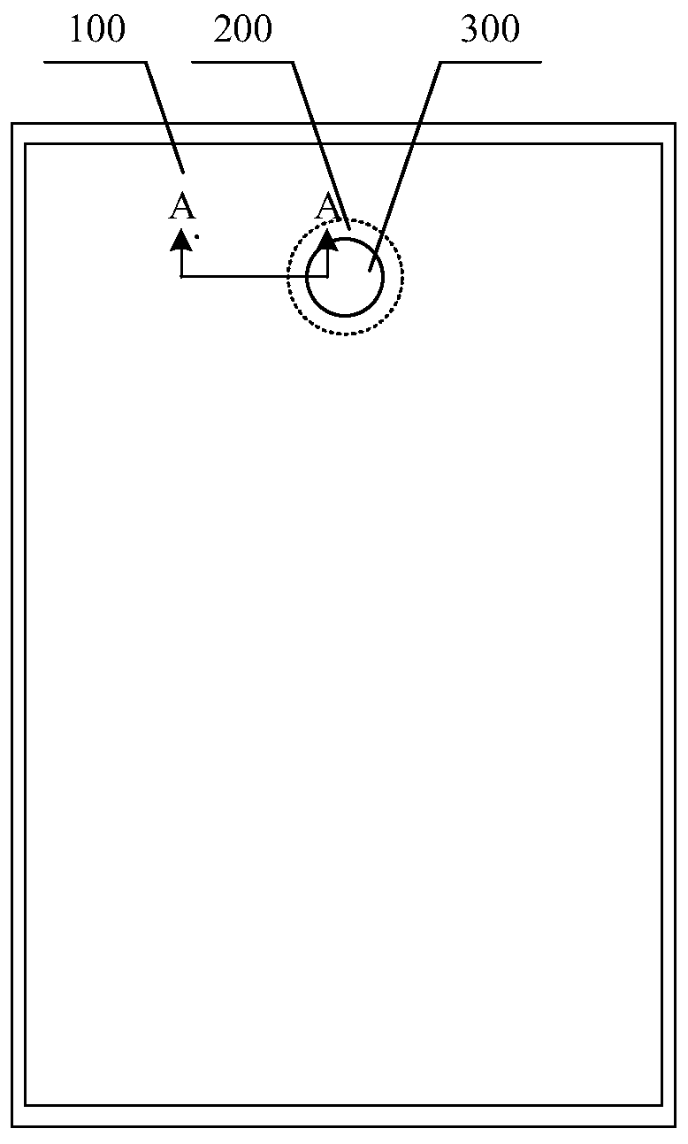
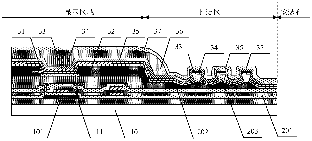
[0061] figure 1 It is a schematic diagram showing the structure of the first embodiment of the substrate of the present invention, figure 2 for figure 1 The cross-sectional view in the direction of A-A in the middle shows the structures of the display area, packaging area and mounting holes on a plane perpendicular to the display substrate. Such as figure 1 As shown, on a plane parallel to the display substrate, the main structure of the display substrate includes a display area 100, a packaging area 200 and a mounting hole 300, the mounting hole 300 is located in the display area 100, and the packaging area 200 is located between the display area 100 and the mounting hole 300 Between is an annular area surrounding the installation hole 300 . The position of the mounting hole 300 in the display area 100 is not limited, and the shape is not limited, it can be figure 1 The circle shown in , can also be other polygons such as ellipse or square, rhombus.
[0062] Such as f...
no. 2 example
[0090] Figure 16 It is a schematic structural diagram of the second embodiment of the display substrate of the present invention, showing the structures of the display area, packaging area and mounting holes on a plane perpendicular to the display substrate. The main structure of the display substrate of this embodiment is basically the same as that of the aforementioned first embodiment, and different from the aforementioned first embodiment, the display substrate of this embodiment is further provided with a filling layer. Such as Figure 16 As shown, on a plane parallel to the display substrate, the main structure of the display substrate includes a display area 100, a packaging area 200 and a mounting hole 300, the mounting hole 300 is located in the display area 100, and the packaging area 200 is located between the display area 100 and the mounting hole 300 Between is an annular area surrounding the installation hole 300 . On a plane perpendicular to the display subst...
no. 3 example
[0095] Based on the technical idea of the embodiment of the present invention, the embodiment of the present invention also provides a method for preparing a display substrate. The display substrate includes a display area, a mounting hole located in the display area, and a packaging area located between the display area and the mounting hole. The method for preparing the display substrate in the embodiment of the present invention includes:
[0096] S1. Forming an insulating layer disposed on the substrate and an encapsulation pixel definition layer disposed on the insulating layer in the encapsulation region, the encapsulation pixel definition layer comprising a plurality of protrusions arranged at intervals;
[0097] S2. Forming an isolation structure layer on the encapsulation pixel definition layer, the isolation structure layer comprising a plurality of pillars arranged at intervals, and the pillars are arranged on the protrusions;
[0098] S3. Forming a functional lay...
PUM
 Abstract
Description
Claims
Application Information
 - Generate Ideas
- Intellectual Property
- Life Sciences
- Materials
- Tech Scout
- Unparalleled Data Quality
- Higher Quality Content
- 60% Fewer Hallucinations
Browse by: Latest US Patents, China's latest patents, Technical Efficacy Thesaurus, Application Domain, Technology Topic, Popular Technical Reports.
© 2025 PatSnap. All rights reserved.Legal|Privacy policy|Modern Slavery Act Transparency Statement|Sitemap|About US| Contact US: help@patsnap.com