Semiconductor testing equipment and working method thereof

A technology of testing equipment and working methods, which is applied in the direction of single semiconductor device testing, semiconductor working life testing, measuring electricity, etc., can solve problems such as easy to generate frost, poor performance of semiconductor testing equipment, and affect testing efficiency, so as to achieve optimal performance, The effect of improving the test yield and reducing the probability of short circuit

Inactive Publication Date: 2019-08-16
HUAIAN IMAGING DEVICE MFGR CORP
View PDF14 Cites 1 Cited by
  • Summary
  • Abstract
  • Description
  • Claims
  • Application Information

AI Technical Summary

Problems solved by technology

[0004] However, during low-temperature testing, the side of the test substrate in the test machine that is not placed on the test product is prone to frost accumulation, which is likely to cause a short circuit and affect the test efficiency, making the performance of the semiconductor test equipment poor.

Method used


Image

  • Semiconductor testing equipment and working method thereof
  • Semiconductor testing equipment and working method thereof
  • Semiconductor testing equipment and working method thereof

Examples


Embodiment Construction

[0027] As described in the background, prior art semiconductor test equipment has poor performance.

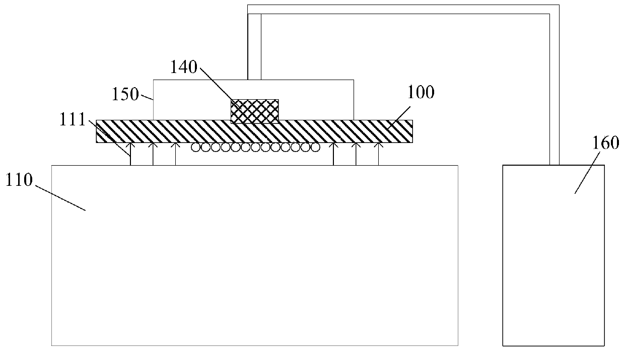
[0028] figure 1 It is a structural schematic diagram of the testing process of a semiconductor testing equipment.

[0029] refer to figure 1 , provide semiconductor test equipment, the semiconductor test equipment includes: a carrier substrate 100, the carrier substrate 100 includes opposite first and second surfaces along the direction of gravity; a test probe 110, the test probe 110 is located on the carrier substrate 100 along the bottom of the gravity direction, the test probe 110 is opposite to the second surface of the carrier substrate 100; the moving device, the moving device drives the test probe 110 to move, so that the test probe 110 is in contact with the second surface of the carrier substrate 100; The sealing cover 150, the sealing cover 150 and the carrier substrate 100 form a sealed cavity; the temperature control mechanism 160 connected with the sealing cove...


PUM


Abstract

The invention discloses a semiconductor testing equipment and a working method thereof. The semiconductor testing equipment comprises a bearing substrate, a testing probe, an air injection component and a movement device, wherein the bearing substrate comprises a first surface and a second surface, and the first surface and the second surface are opposite; the testing probe is provided with a testing end surface, and the testing end surface faces the second surface of the bearing substrate; the air injection component is fixedly connected to the testing end surface and comprises a jet nozzle,the jet nozzle is positioned between the bearing substrate and the testing probe, and the air injection component is used for providing airflow to the second surface of the bearing substrate; and themovement device drives the testing probe to move or drives the bearing substrate to move so as to enable the testing probe to be in contact with the second surface of the bearing substrate. The performance of the semiconductor testing equipment is improved.

Description

technical field [0001] The invention relates to the field of semiconductor testing, in particular to a semiconductor testing device and a working method thereof. Background technique [0002] With the development of modern science and technology and the wide application of electronic products, the reliability index has been compared with the performance, cost, volume, weight and other indicators of electronic products, and has become one of the main indicators to measure the quality of electronic products. The so-called reliability refers to the The ability to perform a specified function under specified conditions and within a specified time. [0003] Electronic components are the basic components of electronic products. However, the use environment of electronic products is relatively complex. Various harsh factors such as temperature, vibration, humidity, shock, and grid voltage fluctuations have a great impact on the performance of electronic products. For temperature fa...

Claims


Application Information

Patent Timeline
Patent Type & Authority Applications(China)
IPC IPC(8): G01R31/26
CPCG01R31/2601G01R31/2642
Inventor 于岑松侯天宇何雪纯高翔
Owner HUAIAN IMAGING DEVICE MFGR CORP
Why Eureka
Try Eureka