Fingerprint sensing device and electronic equipment

A technology for sensing devices and fingerprints, applied in the acquisition/organization of fingerprints/palmprints, circuits, electrical components, etc., can solve the problems of performance degradation of fingerprint sensing devices, damage to semiconductor components, functional failures, etc., to improve electrostatic protection capabilities , the effect of reducing parasitic capacitance and improving capability

Pending Publication Date: 2019-08-16
CHIPONE TECH BEIJINGCO LTD
View PDF0 Cites 1 Cited by
  • Summary
  • Abstract
  • Description
  • Claims
  • Application Information

AI Technical Summary

Problems solved by technology

The voltage difference between the two ends of the above-mentioned electric field increases with the increase of ESD energy. When the voltage difference is greater than the gate breakdown voltage of the semiconductor element, it will cause damage or damage to the semiconductor element, resulting in reduced performance or functional failure of the fingerprint sensor device.

Method used


Image

  • Fingerprint sensing device and electronic equipment
  • Fingerprint sensing device and electronic equipment
  • Fingerprint sensing device and electronic equipment

Examples


Embodiment Construction

[0050] Various embodiments of the invention will be described in more detail below with reference to the accompanying drawings. In the various drawings, the same elements are denoted by the same or similar reference numerals. For the sake of clarity, various parts in the drawings have not been drawn to scale.

[0051] The specific implementation manners of the present invention will be further described in detail below in conjunction with the accompanying drawings and embodiments.

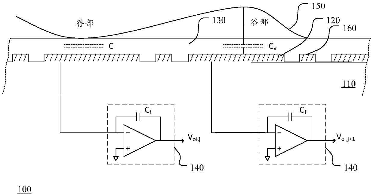
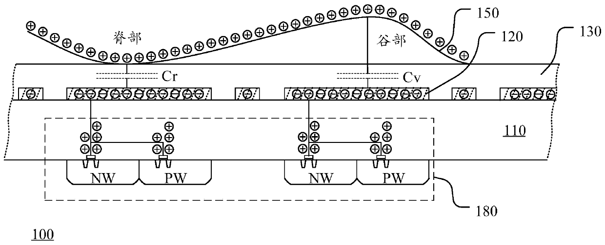
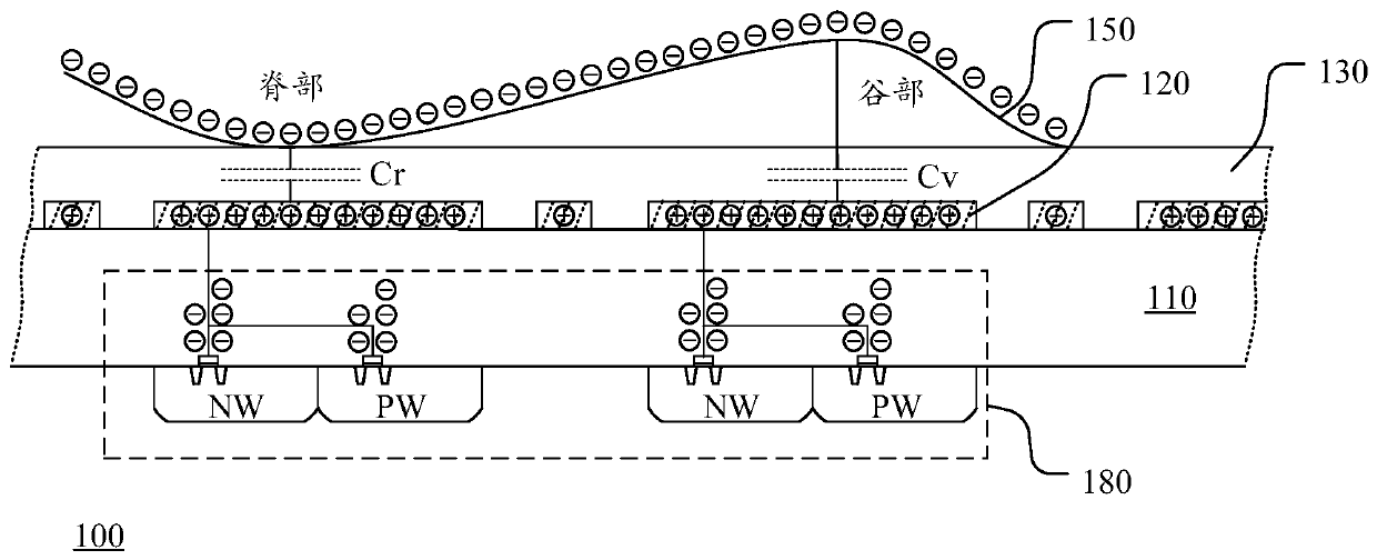
[0052] Figure 4 A schematic diagram of a fourth unit according to the prior art is shown. Such as Figure 4 As shown, the fourth unit 170 of the prior art includes a first diode D1 and a second diode D2 . The fourth unit 170 is used to discharge static electricity and provide conduction paths for normal induction signals and operating currents in the circuit. Preferably, a voltage adjustment module 171 is further included between the first diode D1 and the second diode D2, and the first end of...


PUM


Abstract

The invention discloses a fingerprint sensing device which comprises a first unit, a plurality of second units located on the first unit, and a plurality of fourth units connected to the correspondingsecond units and used for providing a release path of electrostatic charges and a conduction path of sensing signals, wherein each fourth unit includes a voltage adjustment module. By introducing thevoltage adjustment modules to the fingerprint sensing device, the area occupied by the fourth units is reduced, the fourth units can be connected to the corresponding second units respectively, and the electrostatic protection capability of the fingerprint sensing device is improved.

Description

technical field [0001] The invention relates to the technical field of integrated circuits, and more specifically, to a fingerprint sensing device and electronic equipment. Background technique [0002] The prior art fingerprint sensing device has a plurality of second units. When a user places a finger on the surface of the fingerprint sensing device, the variation of the capacitance of the second units is used to determine the pattern of the fingerprint. [0003] figure 1 A schematic diagram of a fingerprint sensing device according to the prior art is shown. Such as figure 1 As shown, the fingerprint sensing device 100 includes a first unit 110 , a second unit 120 located on the first unit 110 , and a protective layer 130 covering the second unit 120 . A third unit 140 connected to the second unit 120 is formed on the first unit 110, and the second unit 120 includes a plurality of second units 120 arranged in a matrix. When the finger 150 touches or approaches the pro...

Claims


Application Information

Patent Timeline
Patent Type & Authority Applications(China)
IPC IPC(8): H01L27/02G06K9/00
CPCH01L27/0255G06V40/1306
Inventor 赵帆李卓陈飞祥
Owner CHIPONE TECH BEIJINGCO LTD
Why Eureka
Try Eureka