X-ray sensor and manufacturing method thereof

A sensor and X-ray technology, applied in the field of sensors, can solve problems such as high cost, crosstalk, and reduced line pair resolution, and achieve the effects of high contrast, clear image quality, and low crosstalk.

Inactive Publication Date: 2019-08-16
NANJING DETECH FUTURE TECH CO LTD
View PDF2 Cites 2 Cited by
  • Summary
  • Abstract
  • Description
  • Claims
  • Application Information

AI Technical Summary

Problems solved by technology

[0005] The existing cesium iodide is formed into a film by thermal evaporation. Although the efficiency is low and the cost is high, the needle-like structure of cesium iodide can transmit the visible light converted by X-rays into the pixel unit of the corresponding photoelectric conversion layer.
At present, perovskite materials are directly coated by solution, which has the advantage of low cost, but the whole surface coating, the X-rays irradiated in a specific area, and the converted visible light easily affect the pixel area of ​​the surrounding photoelectric conversion layer, which is easy to cause crosstalk. Affects the image quality of digital imaging and reduces line pair resolution

Method used


Image

  • X-ray sensor and manufacturing method thereof
  • X-ray sensor and manufacturing method thereof
  • X-ray sensor and manufacturing method thereof

Examples


Embodiment Construction

[0028] Below in conjunction with accompanying drawing and specific embodiment, further illustrate the present invention, should be understood that these embodiments are only for illustrating the present invention and are not intended to limit the scope of the present invention, after having read the present invention, those skilled in the art will understand various aspects of the present invention Modifications in equivalent forms all fall within the scope defined by the appended claims of this application.

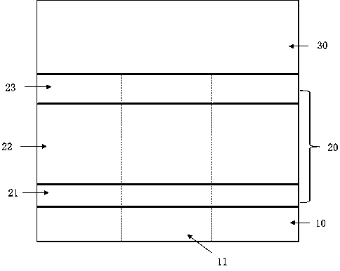
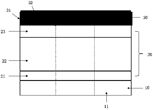
[0029] In order to make the drawing concise, each drawing only schematically shows the parts related to the present invention, and they do not represent the actual structure of the product. In addition, to make the drawings concise and easy to understand, in some drawings, only one of the components having the same structure or function is schematically shown, or only one of them is marked. Herein, "a" not only means "only one", but also means "more than one".

[0030] ...


PUM


Abstract

The invention provides an X-ray sensor and a manufacturing method thereof and belongs to the technical field of sensors. The X-ray sensor includes an array substrate layer, a photoelectric conversionlayer on the array substrate layer, and a scintillator layer. The array substrate layer is provided with array pixel units, and the photoelectric conversion layer is provided with photoelectric pixelunits disposed corresponding to the array pixel units. The scintillator layer includes a plurality of retaining walls and scintillators formed by perovskite solutions in the retaining walls. The retaining walls are corresponding to the photoelectric pixel units and do not exceed the sizes of the photoelectric pixel units. The scintillators are applied or printed on the photoelectric conversion layer. According to the X-ray sensor and the manufacturing method thereof of the invention, the problem of crosstalk between pixels caused by the direct application of a perovskite solution on the surface of the photoelectric conversion layer is solved, and the effects of small crosstalk, clear picture quality and high resolution can be achieved through the invention.

Description

technical field [0001] The invention relates to the technical field of sensors, in particular to an X-ray sensor and a manufacturing method thereof. Background technique [0002] Cosmic rays such as X-rays, γ-rays, and β-rays widely exist in all aspects of daily life, especially X-rays are widely used in medical treatment, security inspection, industrial flaw detection, scientific research and other fields. X-ray detection and sensing technology was invented in the 1990s and is mainly used in X-ray digital imaging (Digital Radiography, DR) technology, which can realize micron-level pixel imaging. [0003] figure 1 It is a structure of an existing X-ray sensor substrate, which includes an array substrate layer 10 , a photoelectric conversion layer 20 and a scintillator layer 30 arranged in sequence. The array substrate layer 10 includes criss-cross scan lines and data lines, a plurality of pixel units 11 defined by intersections of scan lines and data lines, TFT switches lo...

Claims


Application Information

Patent Timeline
Patent Type & Authority Applications(China)
IPC IPC(8): H01L27/146G01T1/00
CPCG01T1/003H01L27/14609H01L27/1462H01L27/14663H01L27/14685
Inventor 陈钢
Owner NANJING DETECH FUTURE TECH CO LTD
Why Eureka
Try Eureka