Supercharge Your Innovation With Domain-Expert AI Agents!

Nitride semiconductor light emitting element

A technology of nitride semiconductors and light-emitting elements, which is applied in semiconductor devices, electrical components, circuits, etc., can solve the problems of reduced luminous efficiency and achieve the effects of improving luminous efficiency, eliminating differences in lattice constants, and suppressing localization

Inactive Publication Date: 2019-08-16
FUJIAN PRIMA OPTOELECTRONICS CO LTD
View PDF3 Cites 0 Cited by
  • Summary
  • Abstract
  • Description
  • Claims
  • Application Information

AI Technical Summary

Problems solved by technology

In the position close to the threading dislocation, carrier localization occurs, which is one of the reasons for the reduction of luminous efficiency

Method used


Image

  • Nitride semiconductor light emitting element
  • Nitride semiconductor light emitting element

Examples


Embodiment Construction

[0018] The present invention will be further described in detail below in conjunction with the accompanying drawings and specific embodiments.

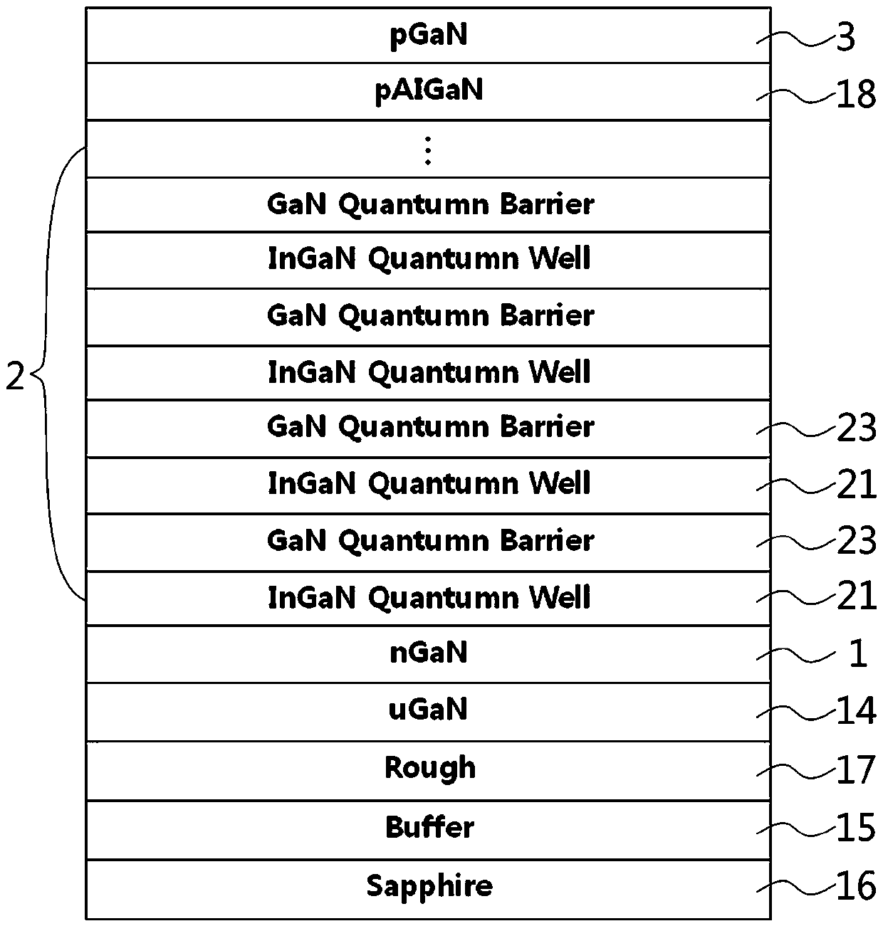
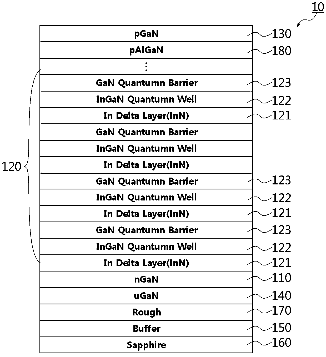
[0019] The invention proposes a new quantum well structure. This quantum well structure can suppress the occurrence of threading dislocations in the light-emitting layer, thereby suppressing the localization of carriers at positions close to the threading dislocations. In general, a GaN-based semiconductor layer has a high density of dislocations generated to eliminate stress due to a difference in lattice constant with a different type of substrate. Such dislocations generate threading dislocations in the light emitting layer. Carrier localization occurs at a site close to threading dislocations, which is one of the causes of reduced luminous efficiency. The quantum well structure of the present invention includes a delta-doped layer disposed under a quantum well layer as a light emitting layer. The delta-doped layer suppresses di...


PUM


Abstract

The invention relates to a nitride semiconductor light emitting element comprising an n-type nitride semiconductor layer; a p-type nitride semiconductor layer; and an active layer which is arranged between the n-type nitride semiconductor layer and the p-type nitride semiconductor layer. The active layer comprises at least one quantum well structure formed by a delta-doped layer, a quantum well layer and a quantum barrier layer which are sequentially laminated. The element is favorable for suppressing penetration dislocation in the light emitting layer and improving the light emitting efficiency.

Description

technical field [0001] The invention relates to the field of light-emitting diodes, in particular to a nitride semiconductor light-emitting element with a multiple quantum well structure. Background technique [0002] Such as figure 1 As shown, the semiconductor light emitting diode generally consists of n-type and p-type doped semiconductor layers (1, 3), and an active layer (2) between them. If driving current is applied to the n-type semiconductor layer (1) and p-type semiconductor layer (3), electrons and holes are injected into the active layer from the n-type semiconductor layer (1) and p-type semiconductor layer (3) respectively (2), the injected electrons and holes recombine in the active layer (2) to emit light. In order to improve the luminous efficiency, a multiple quantum well structure is adopted in the active layer (2). The multiple quantum well structure is a structure in which well layers (21) and potential barrier layers (23) are alternately stacked. [...

Claims


Application Information

Patent Timeline
IPC IPC(8): H01L33/06H01L33/32H01L33/14
CPCH01L33/06H01L33/14H01L33/32
Inventor 吴永胜汪雪琴刘德意
Owner FUJIAN PRIMA OPTOELECTRONICS CO LTD
Features
  • R&D
  • Intellectual Property
  • Life Sciences
  • Materials
  • Tech Scout
  • Unparalleled Data Quality
  • Higher Quality Content
  • 60% Fewer Hallucinations
Learn More