Preparation method of monocrystal piezoelectric film heterogeneous substrate

A heterogeneous substrate, single crystal piezoelectric technology, applied in the direction of piezoelectric/electrostrictive/magnetostrictive devices, circuits, electrical components, etc., can solve the problems of huge gap in thermal expansion coefficient, support substrate fragmentation, etc. Achieve the effect of avoiding the split problem and solving the thermal mismatch problem

Active Publication Date: 2019-08-16
SHANGHAI NOVEL SI INTEGRATION TECH CO LTD
View PDF5 Cites 18 Cited by
  • Summary
  • Abstract
  • Description
  • Claims
  • Application Information

AI Technical Summary

Problems solved by technology

Existing single crystal piezoelectric thin film heterogeneous substrates generally include sequentially stacked support substrates, dielectric buried layers, and single crystal piezoelectric thin films. Since the single crystal piezoelectric substrate (such as a lithium niobate piezoelectric substrate with a thermal expansion coefficient of 15.4 or a lithium tantalate piezoelectric substrate with a thermal expansion coefficient of 16) and a supporting substrate (such as a silicon substrate with a thermal expansion coefficient of 2.5 ) has a huge difference in thermal expansion coefficient, during the process of intelligent peeling, the stress caused by thermal mismatch will cause the single crystal piezoelectric substrate and the support substrate to break

Method used


Image

  • Preparation method of monocrystal piezoelectric film heterogeneous substrate
  • Preparation method of monocrystal piezoelectric film heterogeneous substrate
  • Preparation method of monocrystal piezoelectric film heterogeneous substrate

Examples


Embodiment 1

[0049] see figure 1 , the present invention provides a method for preparing a single crystal piezoelectric thin film heterogeneous substrate, the preparation method of the single crystal piezoelectric thin film heterogeneous substrate comprises the following steps:

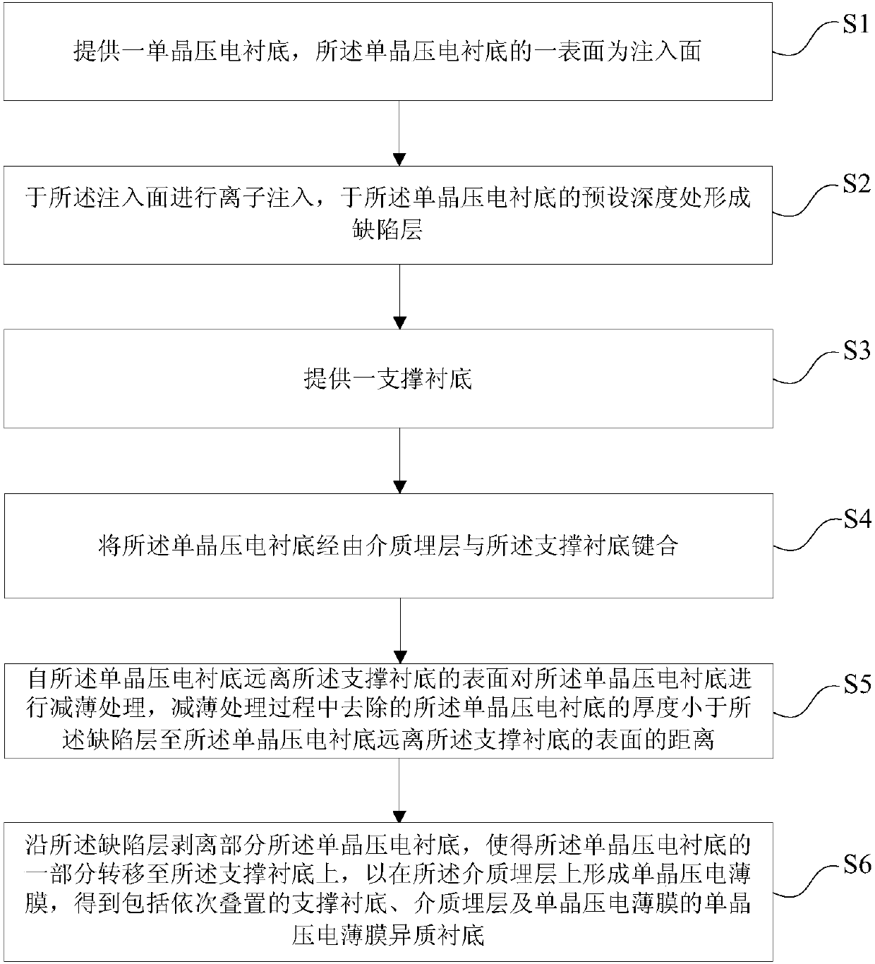
[0050] 1) providing a single crystal piezoelectric substrate, one surface of the single crystal piezoelectric substrate is the injection surface;

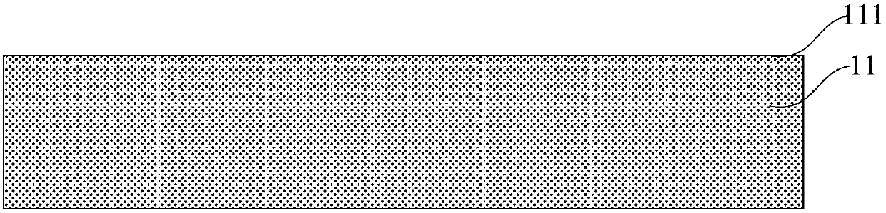
[0051] 2) performing ion implantation on the implanted surface to form a defect layer at a predetermined depth of the single crystal piezoelectric substrate;

[0052] 3) providing a supporting substrate;

[0053] 4) bonding the single crystal piezoelectric substrate to the supporting substrate via a dielectric buried layer;

[0054] 5) Thinning the single crystal piezoelectric substrate from the surface of the single crystal piezoelectric substrate away from the support substrate, and reducing the thickness of the single crystal piezoelectric substrate removed during...

Embodiment 2

[0089] see Figure 12 , the present invention also provides a method for preparing a heterogeneous substrate of a single crystal piezoelectric film, the method for preparing a heterogeneous substrate of a single crystal piezoelectric film described in this embodiment is the same The preparation method of the electric thin film heterogeneous substrate is roughly the same, the difference between the two is that this implementation includes the step of forming the high-sonic material layer 15 on the basis of the first embodiment.

[0090] It should be noted that when the buried dielectric layer 14 is formed on the supporting substrate 13, before the buried dielectric layer 14 is formed on the supporting substrate 13, the buried dielectric layer 14 is formed on the surface of the supporting substrate 13. The high-sonic material layer 15, the dielectric buried layer 14 is formed on the surface of the high-sonic material layer 15; when the dielectric buried layer 14 is formed on the...


PUM


Abstract

The invention provides a preparation method of a monocrystal piezoelectric film heterogeneous substrate. The method comprises the following steps of: 1) providing a monocrystal piezoelectric substrate, wherein one surface of the monocrystal piezoelectric substrate is an implantation surface; 2) performing ion implantation at the implantation surface, and forming a defect layer at the preset depthof the monocrystal piezoelectric substrate; 3) providing a support substrate; 4) bonding the monocrystal piezoelectric substrate with the support substrate through a dielectric buried layer; 5) performing thinning treatment of the monocrystal piezoelectric substrate from the surface, far away from the support substrate, of the monocrystal piezoelectric substrate; and 6) stripping part of the monocrystal piezoelectric substrate along the defect layer to obtain a monocrystal piezoelectric film heterogeneous substrate comprising the support substrate, the dielectric buried layer and the monocrystal piezoelectric film which are stacked in order. The monocrystal piezoelectric substrate is thinned prior to forming of the monocrystal piezoelectric film heterogeneous substrate through stripping along the defect layer, and then stripping is performed along the defect layer to reduce the thermal mismatching between the monocrystal piezoelectric substrate and the support substrate and avoid generation of the problem of cracking caused by thermal mismatch in the stripping process.

Description

technical field [0001] The invention belongs to the technical field of substrate preparation, in particular to a method for preparing a single crystal piezoelectric thin film heterogeneous substrate. Background technique [0002] SAW (Surface Acoustic Wave) and BAW (Body Surface Wave) filters are the only solution for Sub-6GHz mobile communication filters. SAW filters combine low insertion loss and good rejection performance at low cost. However, SAW filters are generally only suitable for applications below 2GHz, and are easily affected by temperature changes (the development of TC-SAW is to solve this problem) and have low power density. BAW (FBAR) filters have excellent performance in high-frequency applications and high power density, and are suitable for very demanding high-frequency signal filtering of 4G and 5G communications. In current RF front-end systems, SAW and BAW (FBAR) filters are used in combination to achieve filtering together. [0003] In the 5G commun...

Claims


Application Information

Patent Timeline
Patent Type & Authority Applications(China)
IPC IPC(8): H01L41/312
CPCH10N30/072
Inventor 欧欣鄢有泉黄凯游天桂王曦
Owner SHANGHAI NOVEL SI INTEGRATION TECH CO LTD
Why Eureka
Try Eureka