Preparation Method of Single Crystal Piezoelectric Thin Film Heterogeneous Substrate
A heterogeneous substrate, single crystal piezoelectric technology, applied in piezoelectric/electrostrictive/magnetostrictive devices, circuits, electrical components, etc., can solve problems such as the huge difference in thermal expansion coefficients and the cracking of supporting substrates
- Summary
- Abstract
- Description
- Claims
- Application Information
AI Technical Summary
Problems solved by technology
Method used
Image
Examples
Embodiment 1
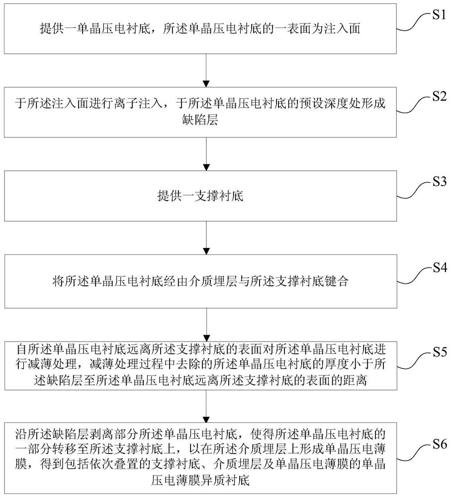
[0049] see figure 1 , the present invention provides a method for preparing a single crystal piezoelectric thin film heterogeneous substrate, the preparation method of the single crystal piezoelectric thin film heterogeneous substrate comprises the following steps:
[0050] 1) providing a single crystal piezoelectric substrate, one surface of the single crystal piezoelectric substrate is the injection surface;
[0051] 2) performing ion implantation on the implanted surface to form a defect layer at a predetermined depth of the single crystal piezoelectric substrate;
[0052] 3) providing a supporting substrate;
[0053] 4) bonding the single crystal piezoelectric substrate to the supporting substrate via a dielectric buried layer;
[0054] 5) Thinning the single crystal piezoelectric substrate from the surface of the single crystal piezoelectric substrate away from the support substrate, and reducing the thickness of the single crystal piezoelectric substrate removed during...
Embodiment 2
[0089] see Figure 12 , the present invention also provides a method for preparing a heterogeneous substrate of a single crystal piezoelectric film, the method for preparing a heterogeneous substrate of a single crystal piezoelectric film described in this embodiment is the same The preparation method of the electric thin film heterogeneous substrate is roughly the same, the difference between the two is that this implementation includes the step of forming the high-sonic material layer 15 on the basis of the first embodiment.
[0090] It should be noted that when the buried dielectric layer 14 is formed on the supporting substrate 13, before the buried dielectric layer 14 is formed on the supporting substrate 13, the buried dielectric layer 14 is formed on the surface of the supporting substrate 13. The high-sonic material layer 15, the dielectric buried layer 14 is formed on the surface of the high-sonic material layer 15; when the dielectric buried layer 14 is formed on the...
PUM
| Property | Measurement | Unit |
|---|---|---|
| thickness | aaaaa | aaaaa |
| thickness | aaaaa | aaaaa |
| thickness | aaaaa | aaaaa |
Abstract
Description
Claims
Application Information


