

A 3D printing packaging method for flip chips
A flip-chip and 3D printing technology, which is applied to semiconductor devices, electrical components, circuits, etc., can solve the problems that flip-chips cannot see the back shape, the thermal conductivity of the insulating layer material is not good, and the overall effect of the lamp is not very good. , to achieve the effect of high degree of freedom, low manufacturing cost, and cost reduction
- Summary
- Abstract
- Description
- Claims
- Application Information
AI Technical Summary
Problems solved by technology
Method used
Image

Examples
Embodiment Construction
[0026] The specific embodiment of the present invention will be further described below in conjunction with accompanying drawing:
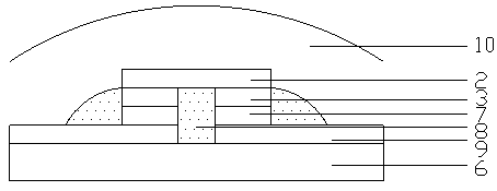
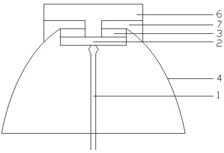
[0027] Such as figure 2 Shown is a schematic cross-sectional view of an embodiment of the present invention. The specific implementation method is carried out as follows:
[0028] S1: Use the computer to design the 3D digital model of the LED device, program the size and material parameters of the LED device, and after layered slice processing, import it into a 3D printer, and the computer controls the printing of each layer;
[0029] S2: Use the suction nozzle (1) to absorb the flip chip (2), and fix it under the reflection cup (4);
[0030] S3: 3D print the solder layer (7) and the heat dissipation substrate (6). The heat dissipation substrate (6) is provided with a lead circuit connected to the chip electrode (3), and each material layer is layered by the 3D printer from bottom to top print it out.
[0031] S4: Fill phosphor powder.
[00...
PUM
 Abstract
Description
Claims
Application Information