Method of forming metal interconnect structure

A technology of metal interconnection structures and metal interconnection lines, which is applied to semiconductor devices, electrical components, circuits, etc., and can solve problems such as extrusion of plugs

Active Publication Date: 2021-06-18
SHANGHAI HUAHONG GRACE SEMICON MFG CORP
View PDF0 Cites 0 Cited by
  • Summary
  • Abstract
  • Description
  • Claims
  • Application Information

AI Technical Summary

Problems solved by technology

[0005] The object of the present invention is to provide a method for forming a metal interconnection structure, so as to solve the problem that the plug is protruded by extrusion

Method used


Image

  • Method of forming metal interconnect structure
  • Method of forming metal interconnect structure
  • Method of forming metal interconnect structure

Examples


Embodiment Construction

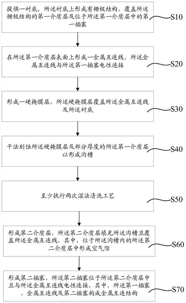
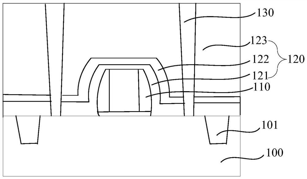
[0032] The method for forming a metal interconnection structure proposed by the present invention will be further described in detail below with reference to the accompanying drawings and specific embodiments. Advantages and features of the present invention will be apparent from the following description and claims. It should be noted that all the drawings are in a very simplified form and use imprecise scales, and are only used to facilitate and clearly assist the purpose of illustrating the embodiments of the present invention. In addition, the structures shown in the drawings are often a part of the actual structure. In particular, each drawing needs to display different emphases, and sometimes uses different scales.

[0033] In the existing semiconductor device manufacturing process, after etching the hard mask layer and the first dielectric layer, before forming the second dielectric layer on the metal interconnection, the grooves between the metal interconnection lines...


PUM


Abstract

The present invention provides a method for forming a metal interconnection structure, comprising: first providing a substrate on which a gate structure, a first dielectric layer and a first plug are formed, and then forming a metal interconnection line and hard mask layer, then etch the hard mask layer and a partial thickness of the first dielectric layer to form grooves, and perform at least two wet cleaning processes on the surface of the grooves and the metal interconnection lines, and then deposit second dielectric layer, so that an air gap is formed in the second dielectric layer in the trench, and finally a second plug is formed in the second dielectric layer, wherein the first plug, the metal interconnection line and the second plug form a metal interconnection structure. Before forming the second dielectric layer, multiple wet cleaning processes are performed on the surface of the groove and the metal interconnection to remove high polymer impurities, so that the gap between the metal interconnection and the subsequently formed second dielectric layer is The stress between them is more balanced, thereby avoiding the risk of the second plug protruding and breaking due to extrusion.

Description

technical field [0001] The invention relates to the technical field of semiconductor manufacturing, in particular to a method for forming a metal interconnection structure. Background technique [0002] With the development of integrated circuits to ultra-large-scale integrated circuits, the circuit density inside integrated circuits is increasing, and the number of components contained is also increasing. This development makes integrated circuits use more than two layers and more than two layers. Layer metal interconnection design. The metal interconnection lines of different layers are electrically connected through plugs. If there are protruding or even broken defects in the plugs, the metal interconnection lines of different layers cannot be electrically connected effectively, so that the products of semiconductor devices are good. rate is greatly reduced. [0003] In addition, during the manufacturing process of the semiconductor structure, when the dielectric layer ...

Claims


Application Information

Patent Timeline
Patent Type & Authority Patents(China)
IPC IPC(8): H01L21/768
CPCH01L21/7682H01L2221/1042
Inventor 邹永金何炳奎曹秀亮
Owner SHANGHAI HUAHONG GRACE SEMICON MFG CORP
Why Eureka
Try Eureka