Transparent display substrate, array substrate, display panel and display device

A transparent display and substrate technology, applied in the direction of diodes, semiconductor devices, electrical components, etc., can solve the problems of not being full screen, not being able to display on the screen, and not being able to display pictures in the camera area

Active Publication Date: 2019-08-20
KUNSHAN GO VISIONOX OPTO ELECTRONICS CO LTD
View PDF5 Cites 36 Cited by
  • Summary
  • Abstract
  • Description
  • Claims
  • Application Information

AI Technical Summary

Problems solved by technology

However, these electronic devices are not truly full-screen, and cannot be displayed in all areas of the entire screen. For example, images cannot be displayed in the camera area.

Method used


Image

  • Transparent display substrate, array substrate, display panel and display device
  • Transparent display substrate, array substrate, display panel and display device
  • Transparent display substrate, array substrate, display panel and display device

Examples


Embodiment Construction

[0077] Reference will now be made in detail to the exemplary embodiments, examples of which are illustrated in the accompanying drawings. When the following description refers to the accompanying drawings, the same numerals in different drawings refer to the same or similar elements unless otherwise indicated. The implementations described in the following exemplary embodiments do not represent all implementations consistent with this application. Rather, they are merely examples of means consistent with aspects of the present application as recited in the appended claims.

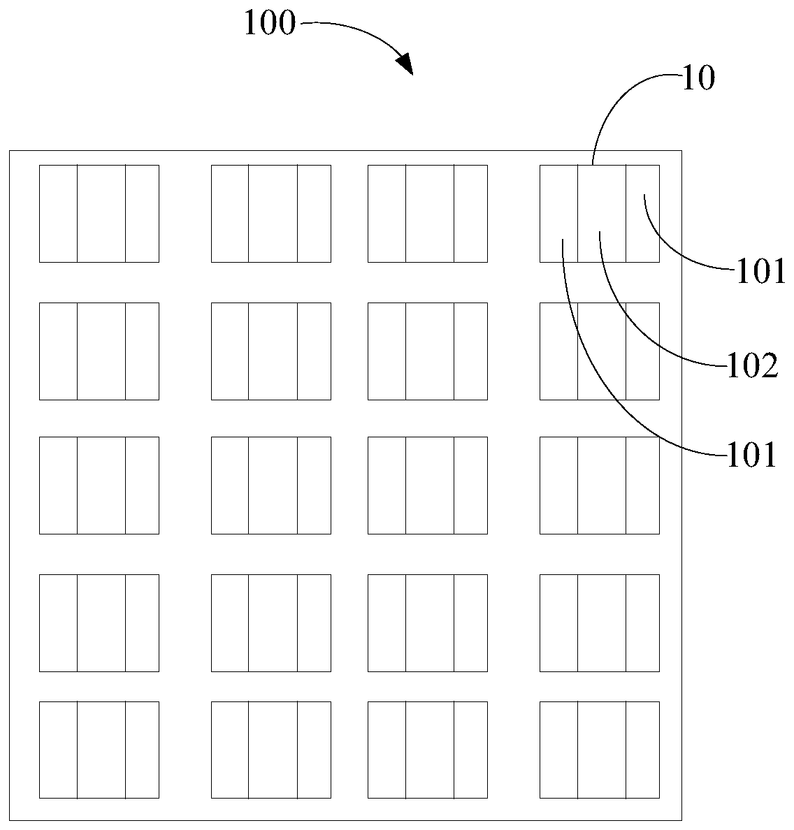
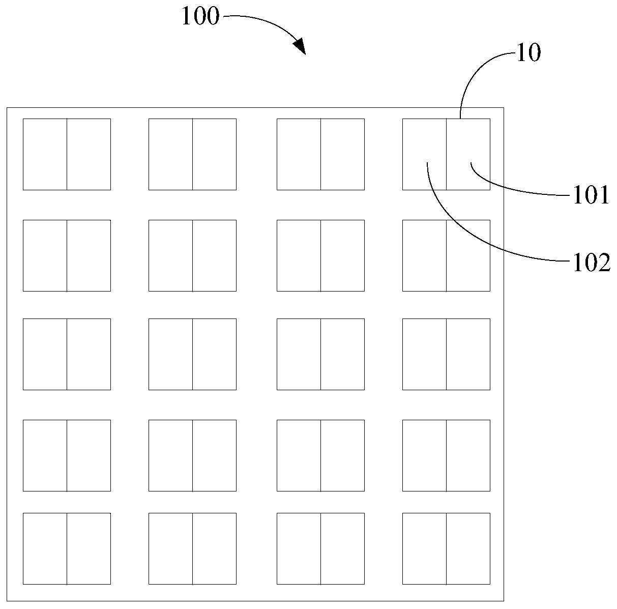
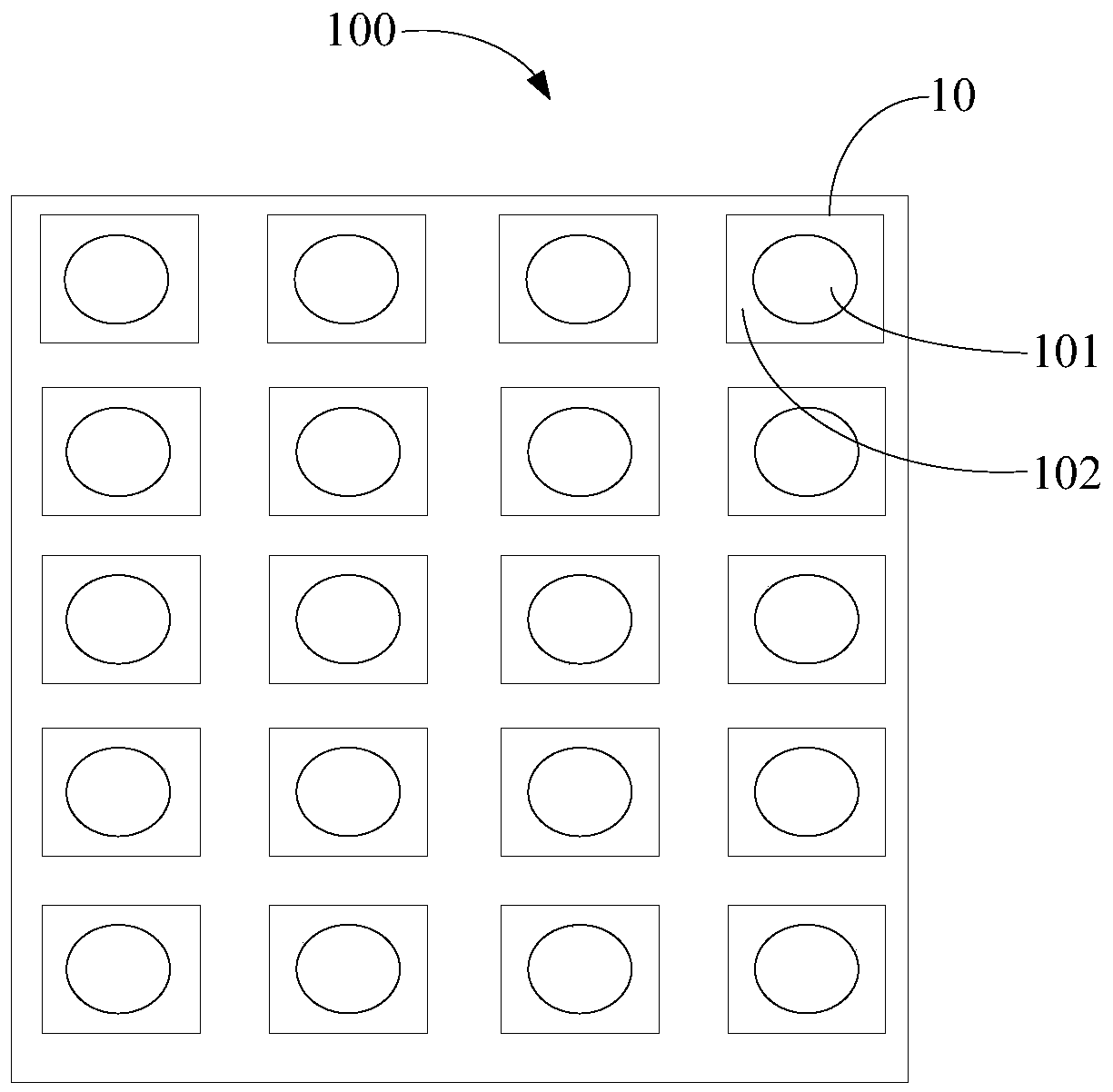
[0078] On smart electronic devices such as mobile phones and tablet computers, due to the need to integrate photosensitive devices such as front cameras and light sensors, the photosensitive devices are generally set in the transparent display area by setting a transparent display area on the above-mentioned electronic devices. Below, the full-screen display of electronic equipment is realized while ensur...


PUM


Abstract

The invention provides a transparent display substrate, an array substrate, a display panel and a display device. A plurality of first sub-pixels are arranged in a display area of the transparent display substrate, wherein each first sub-pixel comprises a first light-emitting area and a second light-emitting area, and the light transmittance of the first light-emitting areas is larger than that ofthe second light-emitting areas. Each first sub-pixel comprises a first electrode, a light-emitting structure located on the first electrode and a second electrode located on the light-emitting structure, wherein the first electrode comprises a first conductive layer and a second conductive layer located on the first conductive layer, and the first conductive layer is in contact with the second conductive layer. One of the first conducting layer and the second conducting layer comprises a reflecting film layer, and the other one of the first conducting layer and the second conducting layer isa transparent conducting film layer, wherein the reflecting film layer is only arranged in the second light-emitting area, and the transparent conducting film layer at least covers the first light-emitting area.

Description

technical field [0001] The present application relates to the field of display technology, in particular to a transparent display substrate, an array substrate, a display panel and a display device. Background technique [0002] With the rapid development of electronic devices, users have higher and higher requirements for screen-to-body ratio, so that the full-screen display of electronic devices has attracted more and more attention from the industry. Traditional electronic devices such as mobile phones, tablet computers, etc., need to integrate such as front camera, earpiece, and infrared sensing components, so it is possible to set the camera, earpiece, and infrared sensing elements in the slotted area by slotting (Notch) on the display screen. Components, etc., but the slotted area cannot be used to display the picture, such as the notch screen in the prior art, or the method of opening holes on the screen. For electronic equipment that realizes the camera function, ext...

Claims


Application Information

Patent Timeline
Patent Type & Authority Applications(China)
IPC IPC(8): H01L27/32H01L51/52
CPCH10K59/00H10K59/353H10K59/65H10K59/12H10K50/805H10K50/852
Inventor 蔡俊飞
Owner KUNSHAN GO VISIONOX OPTO ELECTRONICS CO LTD
Why Eureka
Try Eureka