Power module and semiconductor device
一种功率模块、半导体的技术,应用在半导体器件、半导体/固态器件零部件、电固体器件等方向,能够解决封装体损伤、没有提出间隔件构造、基板应力施加等问题,达到可靠性高的效果
- Summary
- Abstract
- Description
- Claims
- Application Information
AI Technical Summary
Problems solved by technology
Method used
Image

Examples
Embodiment approach 1
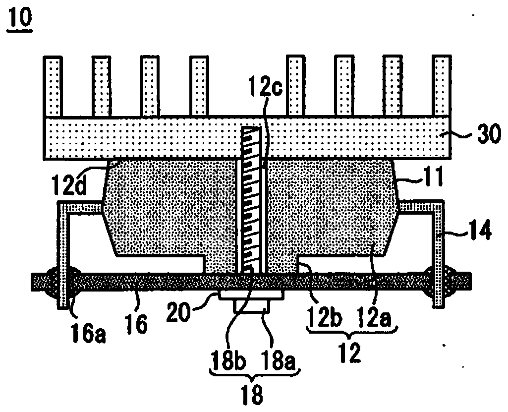
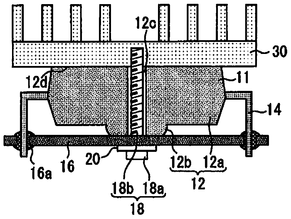
[0038] figure 1 It is a cross-sectional view of the semiconductor device 10 according to the first embodiment. The semiconductor device 10 includes a power module 11 . The power module 11 has semiconductor elements such as IGBTs and diodes inside. The semiconductor element is covered with a resin frame 12 . The resin frame body 12 is provided with the main-body part 12a and the protrusion part 12b. The main body portion 12a is a portion covering the semiconductor element. The protruding portion 12b is a portion protruding from the main body portion 12a. The resin frame 12 is a package of the power module 11 . The lead terminal 14 extends from the main body portion 12a to the outside. The lead terminal 14 is electrically connected to the semiconductor element inside the main body portion 12a.
[0039] The protruding portion 12b is in contact with the printed substrate 16 . Specifically, the bottom surface of the protruding portion 12b is, for example, a flat surface. T...
Embodiment approach 2
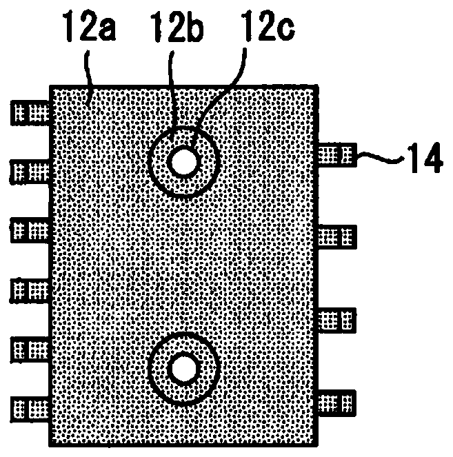
[0048] Figure 6 It is a side view of the semiconductor device according to Embodiment 2. Two protrusions 12b are provided. The resin frame body 12 is provided with the connection part 12e which protrudes from the main-body part 12a, and connects two protrusion parts 12b. The protrusion amount of the connection part 12e from the main body part 12a can be set to the same degree as the protrusion amount of the protrusion part 12b from the main body part 12a. Figure 7 yes Figure 6 The bottom view of the power module 11. For example, by making the width of the connection part 12e approximately the same as the width of the protrusion part 12b, the area of the connection part 12e will not become too large.
[0049] For example, if the power module has a slim shape, if the power module 11 is screwed to the printed circuit board 16 at two places, the central part of the power module 11 may vibrate and resonate, and the resin frame 12 may be damaged. Therefore, in Embodiment 2...
Embodiment approach 3
[0054] Figure 11 It is a cross-sectional view of the semiconductor device according to Embodiment 3. The resin frame body 12 is equipped with the fin 12g which protrudes from the main-body part 12a in the same direction as the protrusion part 12b. The fins 12g are thin flat plates. A plurality of fins 12g can be provided between two protrusions 12b. Figure 12 yes Figure 11 The cross-sectional view at the line B-B'. The width of the fins 12g can be made approximately the same as the width of the main body portion 12a. According to the semiconductor device according to Embodiment 3, heat can be dissipated not only from the heat sink 30 side but also from the surface of the resin housing 12 .
[0055] Figure 13 It is a figure which shows the modification of a fin. The bottom surface of the fin 12h is a curved surface. The fin 12h is provided between the two protrusions, and the amount of protrusion of the fin 12h from the main body 12a can be maximized on the line con...
PUM
 Abstract
Description
Claims
Application Information
 - R&D
- Intellectual Property
- Life Sciences
- Materials
- Tech Scout
- Unparalleled Data Quality
- Higher Quality Content
- 60% Fewer Hallucinations
Browse by: Latest US Patents, China's latest patents, Technical Efficacy Thesaurus, Application Domain, Technology Topic, Popular Technical Reports.
© 2025 PatSnap. All rights reserved.Legal|Privacy policy|Modern Slavery Act Transparency Statement|Sitemap|About US| Contact US: help@patsnap.com