Supercharge Your Innovation With Domain-Expert AI Agents!

A chip packaging structure and packaging method

A chip packaging structure and bare chip technology, applied in the electronic field, can solve problems such as affecting the degree of adhesion of fingerprint chips

Active Publication Date: 2021-08-20
HUAWEI TECH CO LTD
View PDF5 Cites 0 Cited by
  • Summary
  • Abstract
  • Description
  • Claims
  • Application Information

AI Technical Summary

Problems solved by technology

[0004] However, since the upper surface of the bare chip 11 is not coated with the injection molding material 12, when the fingerprint chip is packaged, the bare chip 11 and the injection molding material 12 will shrink under conditions such as high temperature, and the injection molding material 12 with less strength The degree of shrinkage is greater than that of the bare chip 11, so that the packaging structure of the entire bare chip 11 presents a warpage phenomenon with a high center and a low circumference, which affects the degree of bonding between the fingerprint chip and other components.

Method used


Image

  • A chip packaging structure and packaging method
  • A chip packaging structure and packaging method
  • A chip packaging structure and packaging method

Examples


Embodiment Construction

[0049] Hereinafter, the terms "first" and "second" are used for descriptive purposes only, and cannot be understood as indicating or implying relative importance or implicitly specifying the quantity of indicated technical features. Thus, a feature defined as "first" and "second" may explicitly or implicitly include one or more of these features. In the description of the embodiments of the present application, unless otherwise specified, "plurality" means two or more.

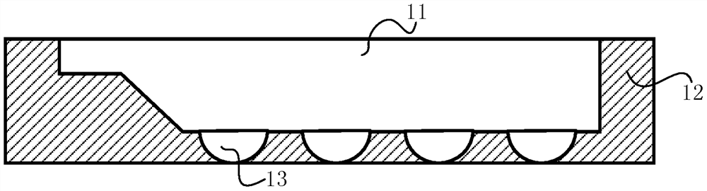
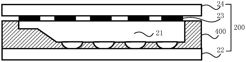
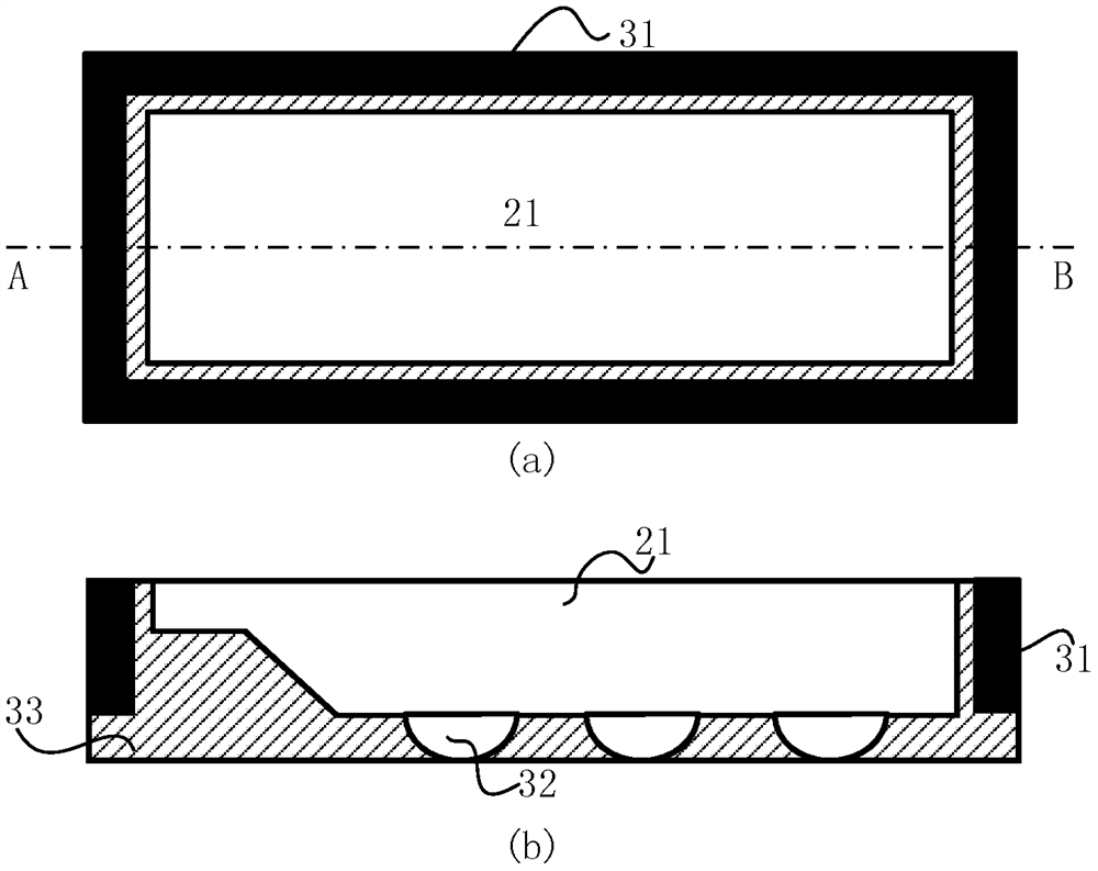
[0050] Embodiments of the present application provide a chip packaging method and a chip packaging structure, which can be applied to the production and use of various chips in a terminal. Take the fingerprint chip as an example, see figure 2 As shown in the cross-sectional view of the fingerprint module 200, the fingerprint chip 21 is packaged to form a chip package structure 400, and the side of the fingerprint chip 21 that includes the solder joints 201 is provided with a soft board 22, such as an FPC sof...


PUM


Abstract

A chip packaging structure (400) and packaging method relate to the field of electronic technology and can improve the warping phenomenon generated when packaging chips. The chip packaging structure (400) includes: a bare chip (41), and a packaging substrate (43) arranged around the bare chip (41), wherein, a solder joint (401) is arranged on the first surface of the bare chip (41) ), the remaining surface of the bare chip (41) except the second surface (402) is wrapped by injection molding material (42), and at least one group of opposite sides of the packaging substrate (43) is embedded in the injection molding material (42), the The contact area between the group of opposite sides and the injection molding material (42) accounts for more than half of the surface area of ​​the group of opposite sides, and the second surface (402) is the surface of the bare chip (41) opposite to the first surface.

Description

technical field [0001] The embodiments of the present application relate to the field of electronic technology, and in particular to a chip packaging structure and a packaging method. Background technique [0002] Chip, also known as microcircuit, microchip or integrated circuit (IC), refers to a silicon chip containing integrated circuits, often a part of terminals such as mobile phones and computers. For example, a fingerprint chip can be set in the mobile phone to realize fingerprint image collection, feature extraction, feature comparison and other fingerprint-related functions, and a display chip can also be set to realize the display function of the terminal display screen. [0003] Generally, after the bare chip (die) is manufactured, it needs to go through the packaging process before it can be used as a chip normally. However, due to the user's demand that the terminal is becoming lighter and thinner, the requirements for the thickness of the package are becoming mo...

Claims


Application Information

Patent Timeline
Patent Type & Authority Patents(China)
IPC IPC(8): H01L23/31H01L21/98
CPCH01L23/31H01L2224/96H01L2924/18162H01L2224/16227H01L2924/3511H01L2924/3512G06V40/1329H01L21/566H01L23/3185H01L23/49838H01L24/13H01L2224/13022G06V40/1318
Inventor 方建平廖彦钦龙浩晖司晖
Owner HUAWEI TECH CO LTD
Features
  • R&D
  • Intellectual Property
  • Life Sciences
  • Materials
  • Tech Scout
  • Unparalleled Data Quality
  • Higher Quality Content
  • 60% Fewer Hallucinations
Learn More