3D NAND storage device and formation method thereof

A 3DNAND, memory technology, applied in semiconductor devices, electro-solid devices, electrical components and other directions, can solve the problem of easy fluctuation of gate spacer feature size and affecting memory performance, etc.

Active Publication Date: 2019-08-27
YANGTZE MEMORY TECH CO LTD
View PDF5 Cites 32 Cited by
  • Summary
  • Abstract
  • Description
  • Claims
  • Application Information

AI Technical Summary

Problems solved by technology

[0004] Existing memories generally include several storage blocks (Block) and several finger storage areas (Fingers) located in the storage block (Block). Between the storage blocks and between the finger storage areas and the finger storage areas, generally pass along the vertical The direction runs through the gate spacer of the stacked structure, but in the manufacturing process of the existing 3D NAND memory, the characteristic size of the gate spacer is easy to fluctuate, which affects the performance of the memory

Method used


Image

  • 3D NAND storage device and formation method thereof
  • 3D NAND storage device and formation method thereof
  • 3D NAND storage device and formation method thereof

Examples


Embodiment Construction

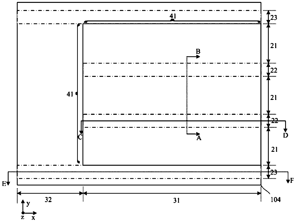
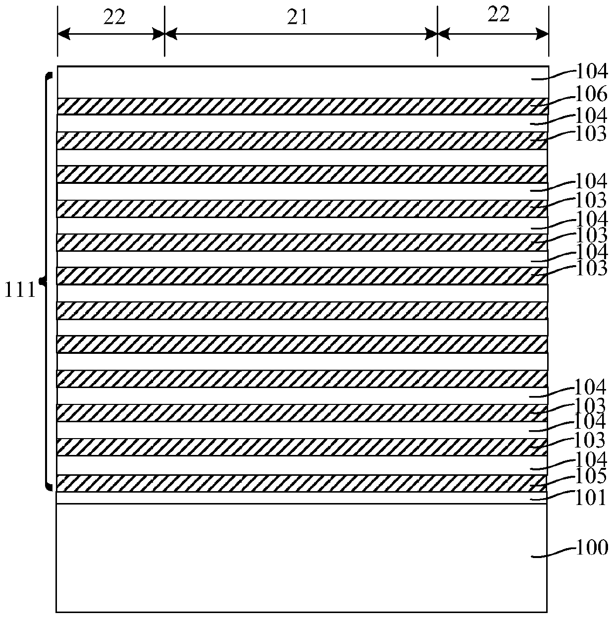
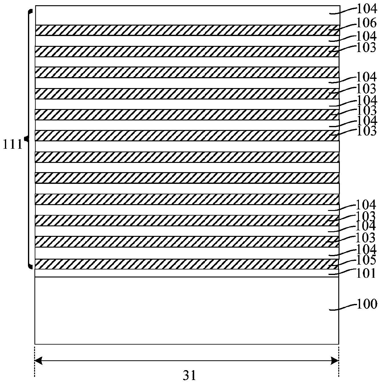
[0043] As mentioned in the background art, in the manufacturing process of the existing 3D NAND memory, the feature size of the gate spacers tends to fluctuate, which affects the performance of the memory.

[0044] It has been found through research that the side walls of the existing gate compartments are prone to inclination, so that the measured characteristic dimensions of the gate compartments tend to fluctuate.

[0045] Further studies have found that due to the large aspect ratio of the formed gate spacer, and after the formation of the gate spacer, the sacrificial layer in the stack structure will be removed, so that the strength of the stack structure is insufficient, which in turn makes the gate spacer The side walls of the groove are easily deformed or inclined. Moreover, since many manufacturing processes in the manufacturing process of 3D NAND memory are carried out at high temperature, the high temperature environment will cause deformation of the isolation layer...


PUM


Abstract

The invention discloses a 3D NAND storage device and a formation method thereof. In the formation method of the 3D NAND storage device, a selective grid sacrificial layer in a first grid partition groove area is disconnected through a first grid partition groove and a plurality of grid partition groove partition areas in the first grid partition groove area, a selective grid sacrificial layer in athrough hole area is disconnected through a selective grid partition area in the through hole area, although the selective grid sacrificial layer on the top of the first grid partition groove area isdisconnected through the first grid partition groove and the grid partition groove partition areas, the sacrificial layer at the bottom of the grid partition groove partition area still remains, namely the sacrificial layers and partition layers in each storage block when the first grid partition groove is formed are still connected together, a stacking structure can be of extremely high supporting strength when the first grid partition groove is formed, and the side wall of the first grid partition groove is unlikely to deform or incline, so that the stability of the feature size of the formed first grid partition groove is guaranteed.

Description

technical field [0001] The invention relates to the field of semiconductor manufacturing, in particular to a method for reducing 3D NAND memory. Background technique [0002] NAND flash memory is a non-volatile storage product with low power consumption, light weight and good performance, and has been widely used in electronic products. At present, the NAND flash memory with a planar structure is close to the limit of practical expansion. In order to further increase the storage capacity and reduce the storage cost per bit, a 3D NAND memory with a 3D structure is proposed. [0003] The formation process of the existing 3D NAND memory generally includes: forming a stacked structure in which isolation layers and sacrificial layers are alternately stacked on the substrate; etching the stacked structure, forming channel vias in the stacked structure, and forming channel vias Finally, etch the substrate at the bottom of the channel via hole to form a groove in the substrate; in ...

Claims


Application Information

Patent Timeline
Patent Type & Authority Applications(China)
IPC IPC(8): H01L27/11575H01L27/11582
CPCH10B43/50H10B43/27H10B43/10H10B43/35
Inventor 霍宗亮欧文杨号号徐伟严萍黄攀周文斌
Owner YANGTZE MEMORY TECH CO LTD
Why Eureka
Try Eureka