
Isolation structure and method for fabricating same

An isolation structure and trench technology, which is used in the manufacture/processing of electromagnetic devices, semiconductor/solid-state device manufacturing, and magnetic field-controlled resistors, etc., can solve problems such as large size, reduce spacing size, maintain isolation effect, and improve The effect of the isolation effect

Active Publication Date: 2019-09-03
UNITED MICROELECTRONICS CORP
View PDF5 Cites 1 Cited by
  • Summary
  • Abstract
  • Description
  • Claims
  • Application Information

AI Technical Summary

Problems solved by technology

However, the size of the shallow trench isolation (STI) structure is still too large

Method used


Image

  • Isolation structure and method for fabricating same
  • Isolation structure and method for fabricating same
  • Isolation structure and method for fabricating same

Examples


Embodiment Construction

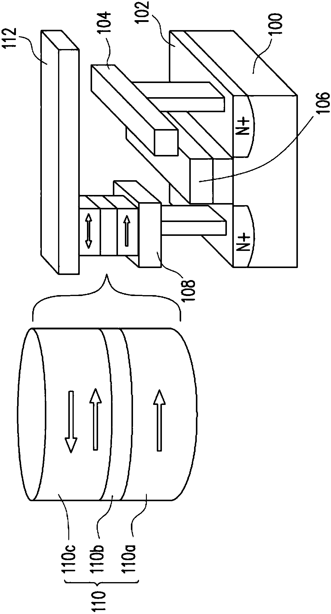
[0062] The present invention relates to isolation techniques for transistors in memory cells of a magnetic random access memory.

[0063] A memory cell at least includes a magnetic tunnel junction (Magnetic Tunnel Junction, MTJ) storage layer and a control transistor. One end of the magnetic tunnel junction storage layer is connected to the drain terminal of the control transistor, and the other end is connected to the bit line. The gate terminal of the control transistor is connected to the word line, and the source terminal is connected to the selection line. Isolation is required between control transistors.

[0064] figure 1 According to an embodiment of the present invention, a schematic diagram of a memory cell structure of a general magnetic random access memory is shown. refer to figure 1, the basic structure of the memory cell of the magnetic random access memory, including the control transistor, which is formed on the substrate 100 . The gate terminal 106 of th...


PUM


Abstract

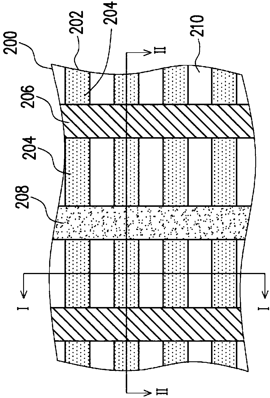
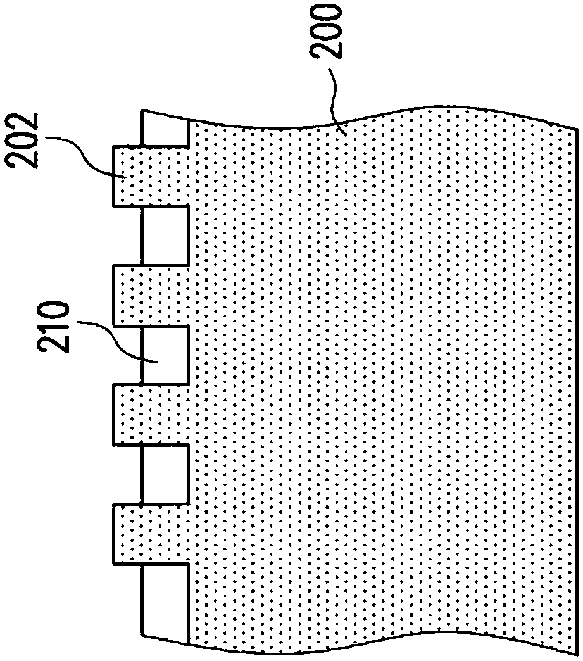
The invention discloses an isolation structure and a method for fabricating the same. The isolation structure is disposed between fin transistors of a magnetic random access memory device and includesa fin line substrate. A trench spans the fin line substrate. An oxide layer is disposed on the fin line substrate outside the trench. A liner layer is disposed on the recessed surface of the trench.A nitride layer is disposed on the liner layer and partially fills the trench. The oxide residue is located on the nitride layer at the bottom within the trench. A gate-like structure is disposed on the oxide layer and completely fills the trench.

Description

technical field [0001] The invention relates to a semiconductor element technology, and in particular to an isolation structure of a semiconductor element and its manufacturing technology. Background technique [0002] Based on the need to reduce the size of semiconductor elements, the design of transistors has undergone considerable research and development. For example, a magnetic random access memory (MRAM) device requires a large number of control transistors. The size of the transistor affects the storage capacity of the memory device. [0003] Regarding the design and development of transistors, for example, fin field effect transistors (fin field effect transistors, FinFETs) have been proposed, which can effectively reduce the size of transistors, which is beneficial to form a part of memory cells of random access memory. [0004] A large number of memory cells are usually planned as a single or multiple memory cell unit, which need to be isolated. For MRAM using f...

Claims


Application Information

Patent Timeline
Patent Type & Authority Applications(China)
IPC IPC(8): H01L43/02H01L43/12
CPCH10N50/80H10N50/01H01L21/76224H01L29/785H10B61/22H01L29/0649H01F10/3254H01L29/7851G11C11/161H01L21/32055H10N50/10
Inventor 朱中良陈昱瑞陈宏岳王裕平
Owner UNITED MICROELECTRONICS CORP
Learn More