A micro-nano optical structure
An optical structure, micro-nano technology, applied in the field of micro-nano optics, can solve the problem of weak circular dichroism signal, and achieve the effects of enhanced chirality, strong practicability, and easy detection.
- Summary
- Abstract
- Description
- Claims
- Application Information
AI Technical Summary
Problems solved by technology
Method used
Image
Examples
Embodiment 1
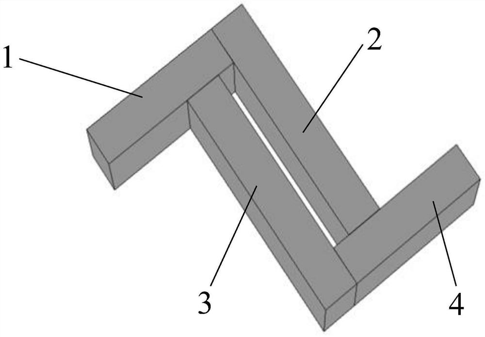
[0032] In order to enhance the circular paramera of natural molecules, the embodiment of the present application provides a micro-nano optical structure, such as figure 1 As shown, including the first metal strip 1, the second metal strip 2, the third metal strip 3, and the fourth metal strip 4, and the second metal strip 2 is connected perpendicular to one end of the first metal strip 1, the third metal strip 3 The second metal strip 2 and the third metal strip 3 are located vertically connected to the other end of the first metal strip 1, and the third metal strip 3 is located in the same side direction of the first metal strip 1. The fourth metal strip 4 is perpendicular to the other end of the third metal strip 3, and the other end of the second metal strip 2 is perpendicular to the non-end position of the other end of the fourth metal strip 4.
[0033] The present application examples provide a microbial optical structure, which can produce a large circular chromaticity, and ...
Embodiment 2
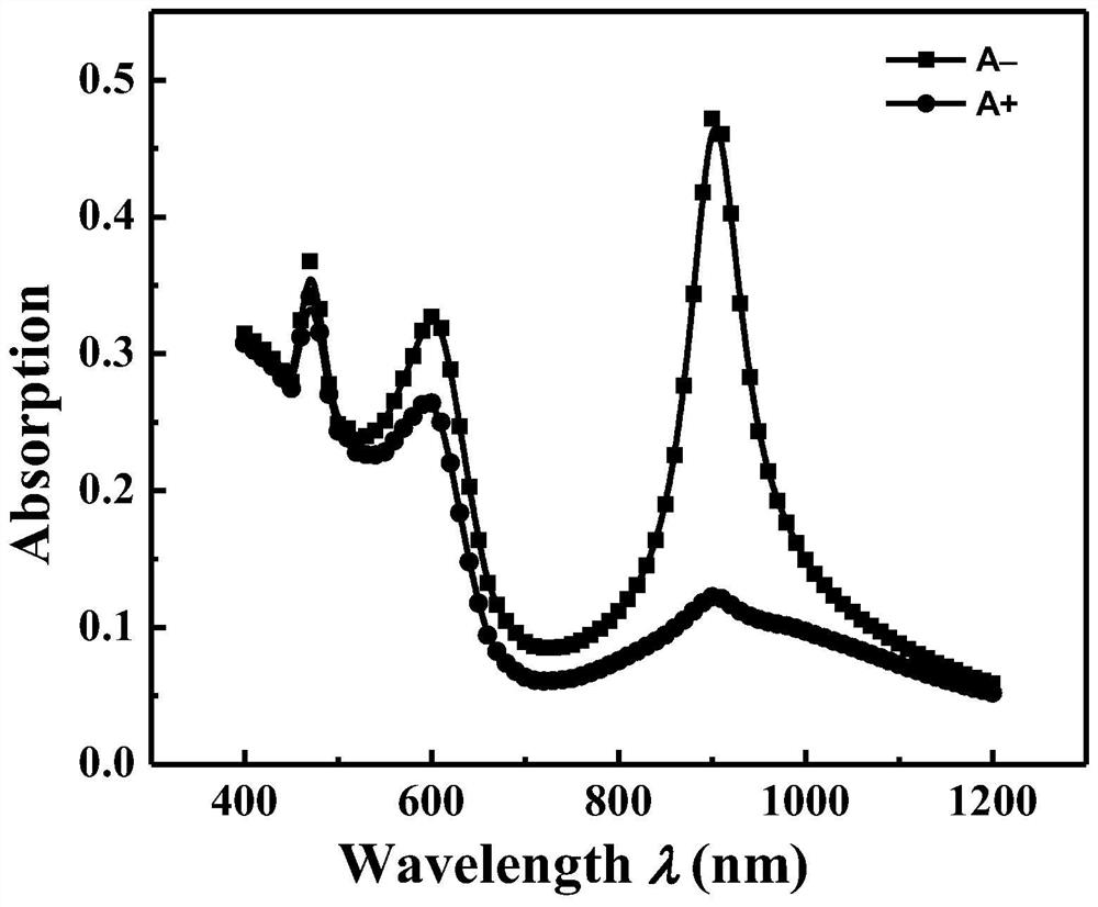
[0037] For further explanation of the circular two color characteristics of the micro-nano optical structure, such as Figure 3 - Figure 6 As shown, the present embodiment discloses its absorption spectrum and a circular dichro spectrogram.
[0038] like figure 1 As shown, the present embodiment sets the micro-ratio optical structure thickness H = 40 nm; the first metal strip 1 length L 1 = Second metal strip 2 length L 2 = Third metal strip 3 length L 3 = Fourth metal strip 4 length L 4 = 100 nm; first metal strip 1 width w 1 = Second metal strip 2 width w 2 = Third metal strip 3 width w 3 = Fourth metal strip 4 width w 4 = 20 nm; the spacing D = 10 nm between the second metal strip 2 and the third metal strip 3.
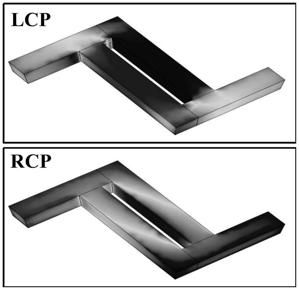
[0039] like figure 2 For the charge distribution map of the present embodiment, from figure 2 In we can see that when the left-handed polarized light (LCP) is irradiated, the positive charge is mainly concentrated on the third metal strip 3, and the negative charge is m...
PUM
| Property | Measurement | Unit |
|---|---|---|
| thickness | aaaaa | aaaaa |
Abstract
Description
Claims
Application Information


