Silicon-based interdigital photoelectric detector

A photodetector, interdigitated technology, applied in circuits, electrical components, semiconductor devices, etc., can solve the problems of small photocurrent and difficult detection of photodetectors, and achieve the effects of simple processing, easy integration, and high modulation efficiency

Active Publication Date: 2019-09-06
HARBIN INST OF TECH SHENZHEN GRADUATE SCHOOL
View PDF5 Cites 9 Cited by
  • Summary
  • Abstract
  • Description
  • Claims
  • Application Information

AI Technical Summary

Problems solved by technology

[0003] In view of the above technical problems, the present invention discloses a silicon-based interdigitated photodetector, which solves the problem that the photoelectric current of the photodetector is too small and difficult to detect

Method used


Image

  • Silicon-based interdigital photoelectric detector
  • Silicon-based interdigital photoelectric detector

Examples


Embodiment Construction

[0027] The preferred embodiments of the present invention will be further described in detail below.

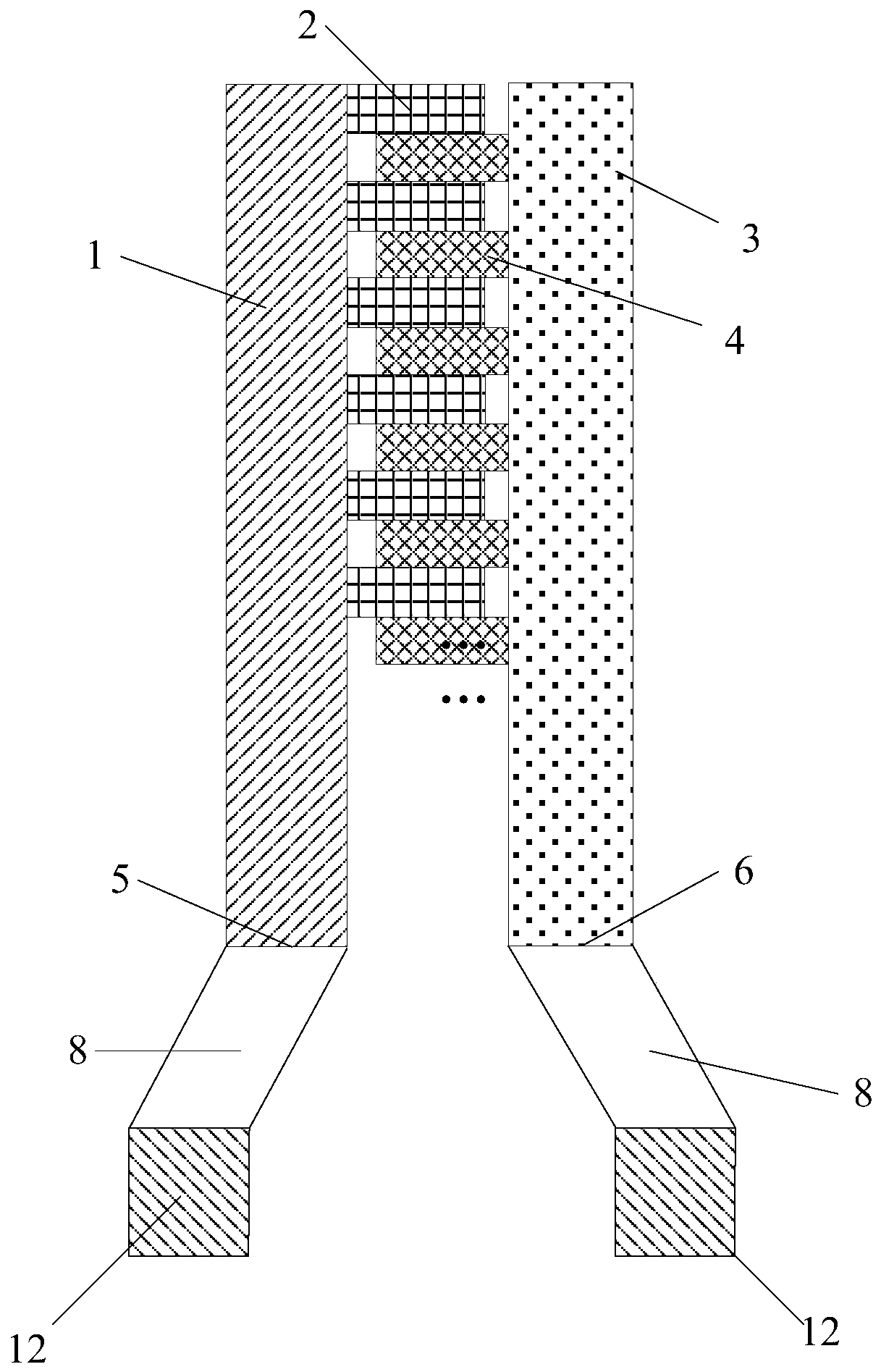
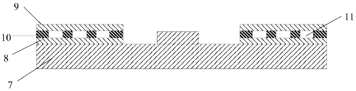
[0028] A silicon-based interdigitated photodetector comprising a substrate 7, a silicon waveguide of an interdigitated structure on the substrate 7 and a metal electrode 12, the silicon waveguide comprising an n-type doped region 1 (i.e. n+ doped region), n-type doped finger 2, p-type doped region 3 (i.e. p+ doped region), p-type doped finger 4, the n-type doped finger 2, p-type doped The fingers 4 are located between the n-type doped region 1 and the p-type doped region 3, the n-type doped fingers 2 and the p-type doped fingers 4 are alternately arranged; the n-type doped The finger 2 is in contact with the n-type doped region 1 on the same side, leaving a gap of 0.2 μm between the p-type doped region 3 on the opposite side; the p-type doped finger 4 is in contact with the p-doped region 3 on the same side The n-type doped region 3 is in contact with the n-type doped region...


PUM


Abstract

The invention provides a silicon-based interdigital photoelectric detector. The silicon-based interdigital photoelectric detector comprises a substrate, a silicon waveguide of an interdigital structure and metal electrodes which are positioned on the substrate, wherein the silicon waveguide comprises an n-type doped region, n-type doped interdigital parts, a p-type doped region, p-type doped interdigital parts, the n-type doped interdigital parts and the p-type doped interdigital parts are positioned between the n-type doped region and the p-type doped region, and the n-type doped interdigitalparts and the p-type doped interdigital parts are arranged alternately; the n-type doped interdigital parts are in contact with the n-type doped region on the same side, and gaps are formed between the n-type doped interdigital parts and the p-type doped region; the p-type doped interdigital parts are in contact with the p-type doped region on the same side, and gaps are formed between the p-typedoped interdigital parts and the n-type doped region; and the metal electrodes are connected with the n-type doped region and the p-type doped region which are positioned on two sides of the waveguide and are connected with the waveguide. Through the technical scheme, electrons jumped to a conduction band from a defect mode energy level due to a defect mode absorption effect can be collected moreefficiently, larger light current is formed, and the performance of the photoelectric detector is improved.

Description

technical field [0001] The invention relates to the technical field of optical signal modulation, in particular to a silicon-based interdigital photodetector. Background technique [0002] In recent years, with the rapid development of optical communication technology, the demand for transmission capacity of optical communication systems continues to increase. But at the same time, optical communication systems with higher transmission capacity have higher requirements for signal transmission, signal modulation and demodulation technology, and signal processing technology, which cannot be met by the slow development of the existing 1550nm band. Such high demands. In order to solve the development bottleneck, people are focusing on the new optical communication system in the 2μm band. The new waveband brings greater development prospects and also brings great challenges. Most of the old optical devices suitable for 1550nm are not suitable for the new 2μm waveband, such as p...

Claims


Application Information

Patent Timeline
Patent Type & Authority Applications(China)
IPC IPC(8): H01L31/101H01L31/0352H01L31/18
CPCH01L31/03529H01L31/101H01L31/1804Y02P70/50
Inventor 徐科孙路路
Owner HARBIN INST OF TECH SHENZHEN GRADUATE SCHOOL
Why Eureka
Try Eureka