
Sieving method of wetting solvent

A screening method and solvent technology, applied in electrical components, semiconductor/solid-state device manufacturing, circuits, etc., can solve the problems of poor photoresist coating uniformity, affecting the quality of integrated circuits, etc., to improve thickness uniformity, reduce light The amount of the inhibitor and the effect of improving the coating condition

Active Publication Date: 2019-09-10
CHANGXIN MEMORY TECH INC
View PDF4 Cites 0 Cited by
  • Summary
  • Abstract
  • Description
  • Claims
  • Application Information

AI Technical Summary

Problems solved by technology

Usually, a large amount of photoresist is required when coating photoresist, and the uniformity of photoresist coating is poor, which affects the quality of integrated circuits

Method used


Image

  • Sieving method of wetting solvent
  • Sieving method of wetting solvent
  • Sieving method of wetting solvent

Examples


Embodiment 1

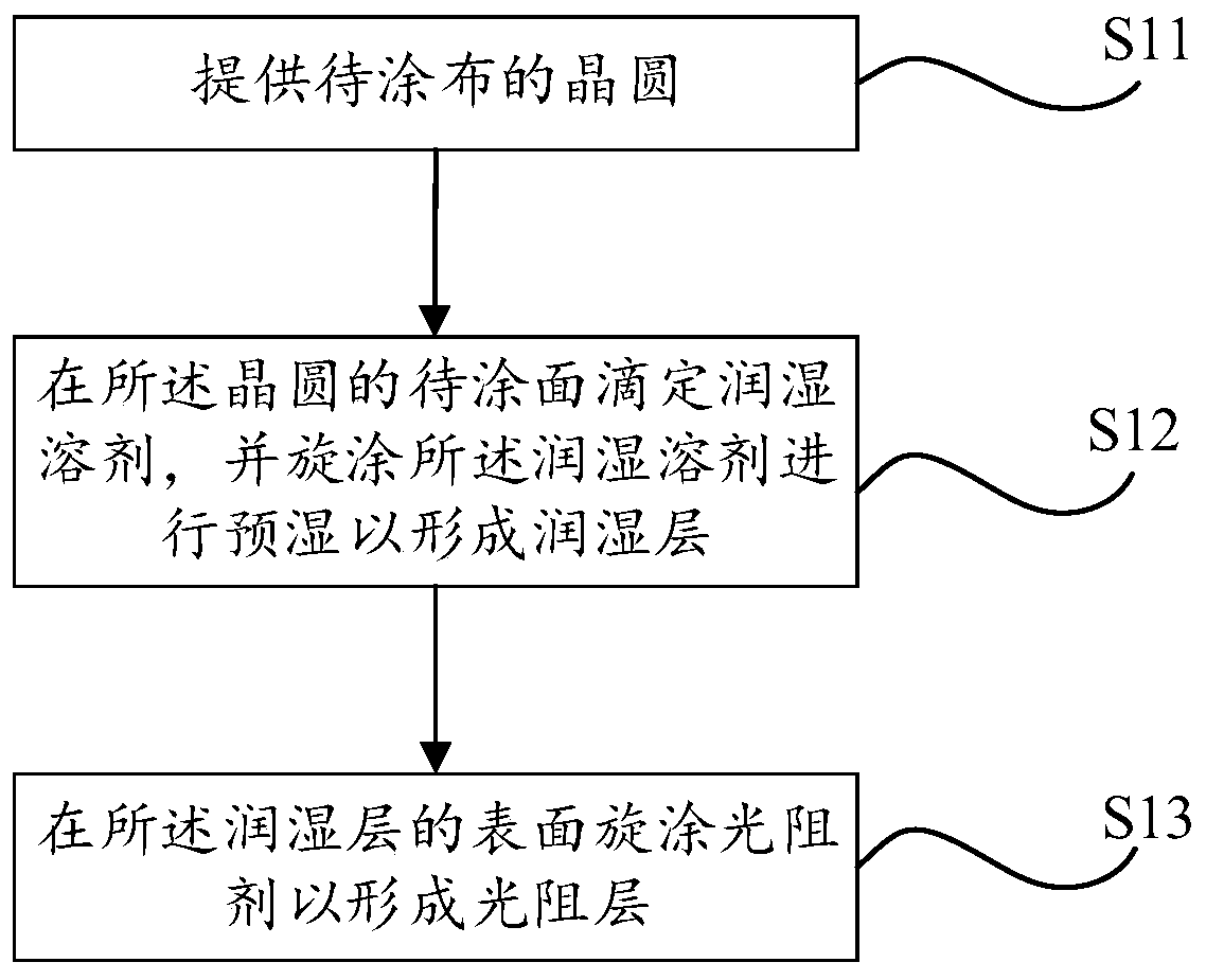
[0057]This embodiment provides a process technology for photoresist coating, such as figure 1 As shown, the process includes:

[0058] Step S11: providing a wafer to be coated;

[0059] Step S12: Titrating a wetting solvent on the surface of the wafer to be coated, and spin coating the wetting solvent for pre-wetting to form a wetting layer;

[0060] Step S13: Spin-coat photoresist on the surface of the wetting layer to form a photoresist layer.

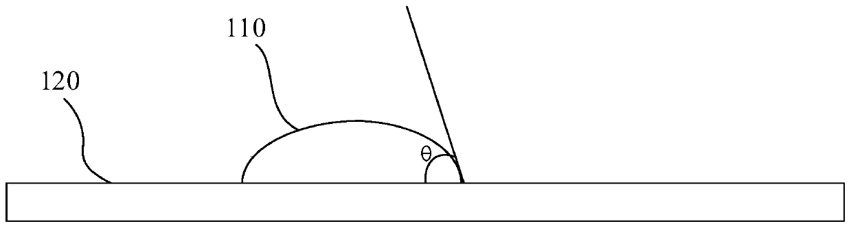
[0061] which, combined with figure 2 As shown, the contact angle between the wetting solvent droplet 110 formed on the surface to be coated of the wafer 120 and the surface to be coated of the wafer 120 by titration of the wetting solvent is θ, and the contact angle θ is measured, and the The contact angle between the wetting solvent droplet 110 formed on the surface to be coated and the surface to be coated of the wafer 120 by wetting solvent titration is less than 90°, that is, θ1 / 2 , the polarity parameter is between 4.1~16.7M...

Embodiment 2

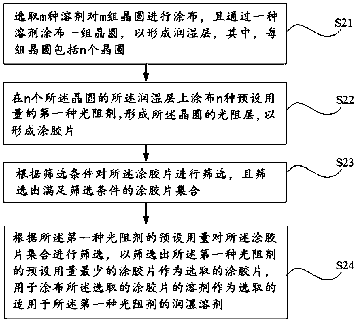
[0079] This embodiment provides a screening method of wetting solvents for coating and wetting the wafer before coating photoresist, such as image 3 As shown in the flow chart, including:

[0080] Step S21: Select m kinds of solvents to coat m groups of wafers, and coat a group of wafers with a solvent to form a wetting layer of the wafers, wherein each group of wafers includes n wafers, m and n are both positive integers greater than or equal to 2;

[0081] Step S22: Coating n types of preset photoresists on the wetting layers of the n wafers to form the photoresist layer of the wafers to form a glue-coated sheet, wherein each group of wafers In the circle, a wafer is coated with a preset amount of the first photoresist to form n types of coated films;

[0082] Step S23: Screening the coated sheets according to the screening conditions, and filtering out a set of coated sheets satisfying the screening conditions;

[0083] Step S24: Screen the set of coated sheets accordin...

Embodiment 3

[0118] This embodiment provides a use of a solvent including cyclohexanone and / or cyclohexanone derivatives for coating and wetting a wafer before coating a photoresist.

[0119] In this embodiment, the solvent comprising cyclohexanone and / or cyclohexanone derivatives is used as a wetting solvent for coating and wetting the wafer before coating the photoresist, so that the photoresist is coated with The wetting solvent is evenly mixed on the contact surface, which improves the uniformity of photoresist coating, and further improves the uniformity of the thickness of the photoresist layer formed by the photoresist.

[0120] Regarding the use of solvents including cyclohexanone and / or cyclohexanone derivatives as coating wetting of wafers prior to coating of photoresist, the applicable range includes ArF dry photolithography and ArF immersion In the photolithography method, the wafer is wetted before coating; wherein, the ArF dry photolithography method is a method of dry photol...


PUM

PropertyMeasurementUnit
polarity parameteraaaaaaaaaa
wavelengthaaaaaaaaaa

Abstract

The invention provides a sieving method of a wetting solvent. The method comprises the steps of selecting m solvents, and coating m groups of wafers; coating n types of first photoresist with preset dosage on wetting layers of the n wafers to form photoresist layers so as to form gluing pieces; sieving the gluing pieces according to a sieving condition, and sieving out a gluing piece set conforming to the sieving condition; and sieving the gluing set according to the preset dosage of the first photoresist so as to sieve out the gluing piece with minimum preset dosage of the first photoresist as a selected gluing piece, wherein the solvent for coating the selected gluing piece is used as the selected wetting solvent applicable to the first photoresist. The wetting solvent for coating and wetting the wafer before photoresist coating is sieved out, thus, the photoresist coating condition of the wafer surface is effectively improved, and the thickness uniformity of the photoresist layers of the gluing pieces is improved.

Description

[0001] This application is a divisional application of a Chinese patent application with the title of "Photoresist Coating Process, Wetting Solvent Screening Method and Wetting Solvent" filed on March 2, 2018, with the application number "201810173987.5". technical field [0002] The invention relates to photoresist coating in the integrated circuit yellow light manufacturing process, in particular to a screening method for a wetting solvent. Background technique [0003] With the improvement of the quality requirements of integrated circuits, in the photoresist coating of the yellow light process with a wafer size of 8 inches and above, it is necessary to maintain the uniformity of the thickness of the photoresist layer formed by the photoresist and reduce the photoresist during the coating process. The amount of resist used is particularly important. Usually, a large amount of photoresist needs to be used when coating the photoresist, and the coating uniformity of the phot...

Claims


Application Information

Patent Timeline
Patent Type & Authority Applications(China)
IPC IPC(8): G03F7/16H01L21/027
CPCG03F7/16H01L21/0273
Inventor 黄帅吴明锋
Owner CHANGXIN MEMORY TECH INC
Learn More