Photoresist coating process, wetting solvent screening method and wetting solvent
A technology of coating process and screening method, which is applied in the direction of photoplate-making process coating equipment, electrical components, semiconductor/solid-state device manufacturing, etc., can solve the problems affecting the quality of integrated circuits, poor uniformity of photoresist coating, etc., to achieve Reduce the amount of photoresist, improve the thickness uniformity, and reduce the cost
- Summary
- Abstract
- Description
- Claims
- Application Information
AI Technical Summary
Problems solved by technology
Method used
Image
Examples
Embodiment 1
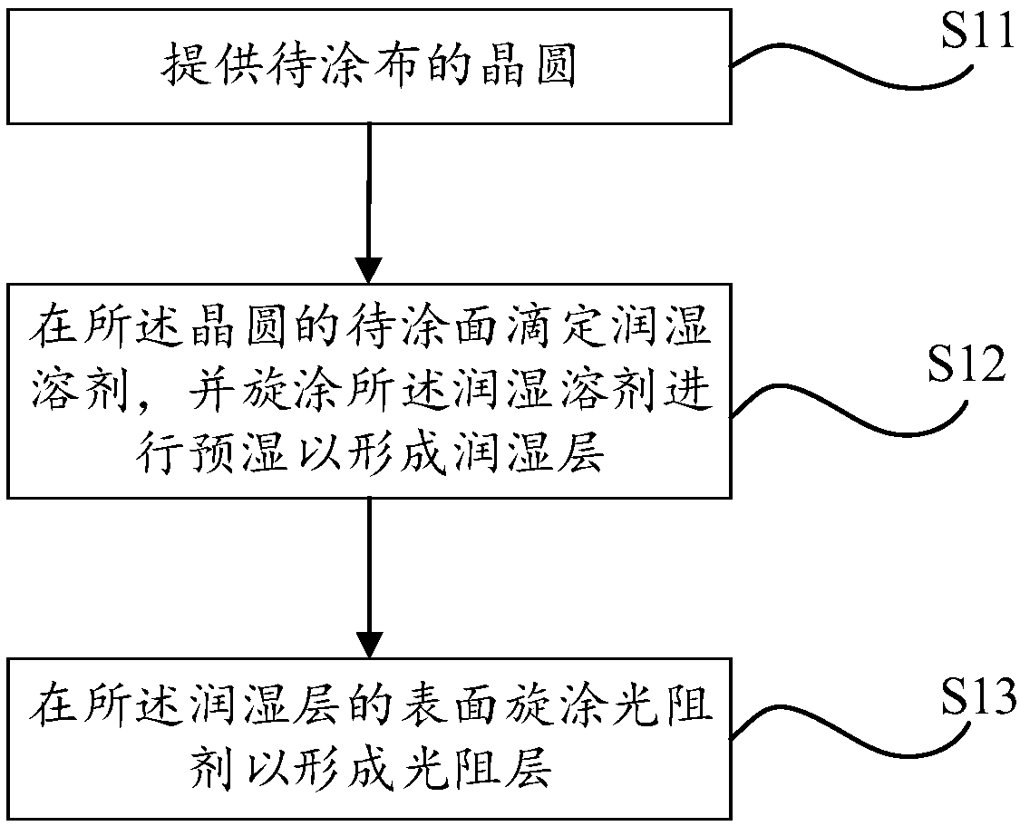
[0059] This embodiment provides a process technology for photoresist coating, such as figure 1 As shown, the process includes:
[0060] Step S11: providing a wafer to be coated;
[0061] Step S12: Titrating a wetting solvent on the surface of the wafer to be coated, and spin coating the wetting solvent for pre-wetting to form a wetting layer;
[0062] Step S13: Spin-coat photoresist on the surface of the wetting layer to form a photoresist layer.
[0063] which, combined with figure 2 As shown, the contact angle between the wetting solvent droplet 110 formed on the surface to be coated of the wafer 120 and the surface to be coated of the wafer 120 by titration of the wetting solvent is θ, and the contact angle θ is measured, and the The contact angle between the wetting solvent droplet 110 formed on the surface to be coated and the surface to be coated of the wafer 120 by wetting solvent titration is less than 90°, that is, θ1 / 2 , the polarity parameter is between 4.1~16.7...
Embodiment 2
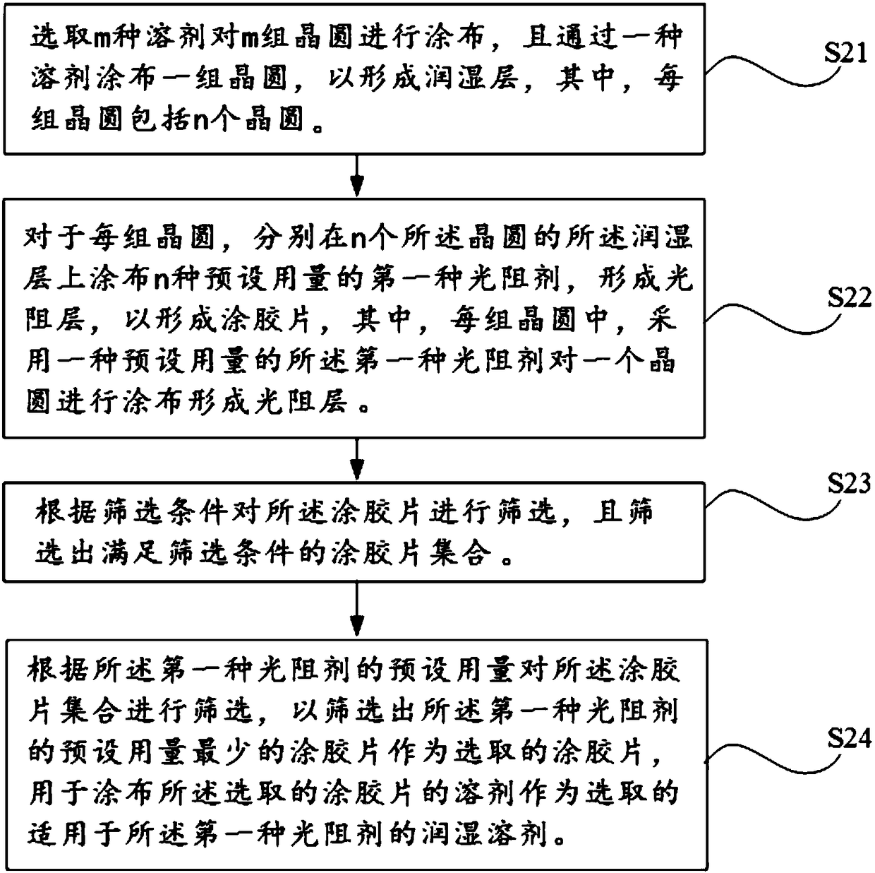
[0081] This embodiment provides a screening method of wetting solvents for coating and wetting the wafer before coating photoresist, such as image 3 As shown in the flow chart, including:
[0082] Step S21: Select m kinds of solvents to coat m groups of wafers, and coat a group of wafers with one solvent to form a wetting layer, wherein each group of wafers includes n wafers, and m and n are equal to is a positive integer greater than or equal to 2;
[0083] Step S22: For each group of wafers, apply n kinds of preset amounts of the first photoresist on the wetting layers of n wafers respectively to form a photoresist layer to form a glue-coated sheet, wherein , in each group of wafers, a wafer is coated with a preset amount of the first photoresist to form a coated film;
[0084] Step S23: Screening the coated sheets according to the screening conditions, and filtering out a set of coated sheets satisfying the screening conditions;
[0085] Step S24: Screen the set of coat...
Embodiment 3
[0120] This embodiment provides a use of a solvent including cyclohexanone and / or cyclohexanone derivatives for coating and wetting a wafer before coating a photoresist.
[0121] In this embodiment, the solvent comprising cyclohexanone and / or cyclohexanone derivatives is used as a wetting solvent for coating and wetting the wafer before coating the photoresist, so that the photoresist is coated with The wetting solvent is evenly mixed on the contact surface, which improves the uniformity of photoresist coating, and further improves the uniformity of the thickness of the photoresist layer formed by the photoresist.
[0122] Regarding the use of solvents including cyclohexanone and / or cyclohexanone derivatives as coating wetting of wafers prior to coating of photoresist, the applicable range includes ArF dry photolithography and ArF immersion In the photolithography method, the wafer is wetted before coating; wherein, the ArF dry photolithography method is a method of dry photol...
PUM
 Abstract
Description
Claims
Application Information


