Flexible SOI device structure and preparation method thereof

A device structure and flexible technology, applied in semiconductor/solid-state device manufacturing, electrical components, transistors, etc., can solve the problems of poor back-gate isolation and complex back-gate device manufacturing process, achieve good isolation, and improve off-state leakage current. Increase and control accurate effects

Inactive Publication Date: 2019-09-10
SHANGHAI INST OF MICROSYSTEM & INFORMATION TECH CHINESE ACAD OF SCI
View PDF4 Cites 2 Cited by
  • Summary
  • Abstract
  • Description
  • Claims
  • Application Information

AI Technical Summary

Problems solved by technology

[0004] The purpose of the present invention is to provide a flexible SOI device structure and its preparation method, so as to solve the problems of complex preparation process and poor back gate isolation in the prior art

Method used


Image

  • Flexible SOI device structure and preparation method thereof
  • Flexible SOI device structure and preparation method thereof

Examples


Embodiment Construction

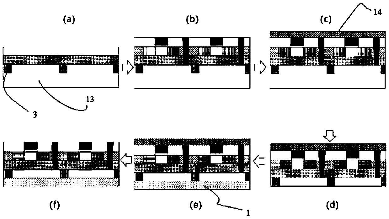
[0035] The present invention will be further described below in conjunction with specific embodiments. It should be understood that the following examples are only used to illustrate the present invention but not to limit the scope of the present invention.

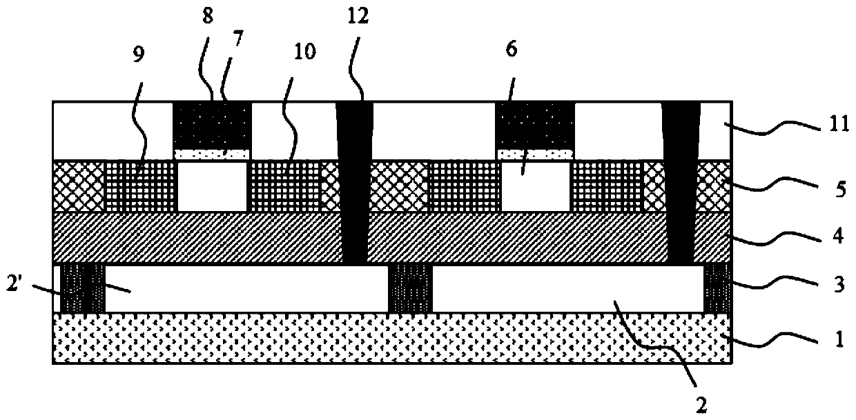
[0036] According to a preferred embodiment of the present invention, a flexible SOI device structure is provided, and the flexible SOI device structure includes in order from bottom to top: a flexible substrate 1; a first back gate region 2 above the flexible substrate 1; Two back gate regions 2' and the back gate isolation part 3; the insulating buried layer 4 located above the first back gate region 2, the second back gate region 2' and the back gate isolation part 3; the insulating buried layer 4 located above The first active region, the second active region, and the device isolation part 5 located at the outer end of the first active region, the second active region and between them, specifically, the first and secon...


PUM


Abstract

The invention provides a flexible SOI device structure and a preparation method thereof; the flexible SOI device structure sequentially comprises a flexible substrate, a first back gate region, a second back gate region and an inter-back-gate isolation part, an insulating buried layer, a first active region, a second active region and a device isolation part, an interlayer dielectric layer and a contact hole from the bottom up, wherein the first back gate region, the second back gate region and the inter-back-gate isolation part are located above the insulating buried layer; each of the firstactive region and the second active region comprises a gate region, a body region located below the gate region, and a source and a drain which are located at the two transverse ends of the body region respectively; the interlayer dielectric layer is located at the highest position; the contact hole runs through the interlayer dielectric layer, the device isolation part and the insulating buried layer in sequence; and the contact hole is filled with a conductive material to form a contact part, and the first back gate region and the second back gate region are applied with a bias voltage by the contact part, wherein the first back gate region and the second back gate region are electrically isolated from each other by the inter-back-gate isolation part. According to the structure, the inter-back-gate isolation part is added to realize independent modulation of the back gate device; and meanwhile, the flexible preparation of the flexible SOI device structure is realized.

Description

technical field [0001] The invention belongs to the technical field of semiconductor manufacturing, and more specifically relates to a flexible SOI device structure and a preparation method thereof. Background technique [0002] Flexible electronic technology has become a research hotspot in the electronics industry and academia because of its outstanding scalability, portability and adaptability. In particular, the combination of silicon-based rigid materials and soft substrates makes electronic devices flexible and extensible while maintaining the original high performance and high reliability, which has engineering application value. Since silicon-on-insulator (SOI, Silicon-on-Insulator) technology introduces an insulating buried layer (BOX, BuriedOxide) between the single crystal silicon device layer and the silicon substrate, complete dielectric isolation is achieved, with latch-up immunity, speed High, low power consumption, high integration, high temperature resistan...

Claims


Application Information

Patent Timeline
Patent Type & Authority Applications(China)
IPC IPC(8): H01L27/088H01L21/8234
CPCH01L21/8234H01L21/823481H01L27/088
Inventor 常永伟董业民吕凯
Owner SHANGHAI INST OF MICROSYSTEM & INFORMATION TECH CHINESE ACAD OF SCI
Why Eureka
Try Eureka