High-power vertical cavity surface emitting laser with integrated light emitting area
A vertical cavity surface emission and laser technology, which is applied in the direction of semiconductor lasers, lasers, laser components, etc., can solve the problem of uneven distribution of laser current density, achieve the effect of increasing power, reducing quantity, and improving conversion efficiency
- Summary
- Abstract
- Description
- Claims
- Application Information
AI Technical Summary
Problems solved by technology
Method used
Image
Examples
Embodiment 1
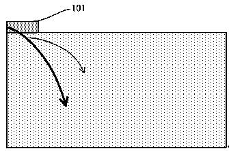
[0040] This embodiment provides a high-power vertical-cavity surface-emitting laser with an integrated light-emitting area. After research and analysis, the existing vertical-cavity surface-emitting laser with a ring-shaped upper electrode structure 113, when the current is injected, the current will mainly concentrate on the emission hole 10 The edge region of the emission hole 10 has a small current or even no current in the middle region of the emission hole 10. The current distribution in the edge region of the emission hole 10 is relatively crowded, while there is almost no current distribution in the middle region, which will cause the overall conversion efficiency of the vertical cavity surface emitting laser to be low. Low, the light intensity distribution in the emission hole 10 is not uniform. The design principle of the present invention is: the elongated emission regions 100 in the emission hole 10 are connected as a whole, and the distance (such as the lateral dist...
Embodiment 2
[0066] Such as Figure 3~Figure 4 As shown, among them, Figure 4 shown as image 3 The schematic diagram of the cross-sectional structure at BB' in the middle, this embodiment provides a high-power vertical cavity surface emitting laser with an integrated light emitting area, its basic structure is as in embodiment 1, wherein the vertical cavity surface emitting laser is a back emitting structure, The vertical cavity surface emitting laser includes: a P-type conductive lower reflector 211, the back of the P-type conductive lower reflector 211 has a lower electrode structure 107; an active layer 109 is located on the P-type conductive lower reflector 211 On; the N-type conductive upper reflector 208, located above the active layer 109, the N-type conductive upper reflector 208 has a current confinement layer 110, and the emission hole 10 is defined by the current confinement layer 110 The substrate 106 is located on the N-type conductive upper mirror 208; the dielectric laye...
Embodiment 3
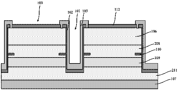
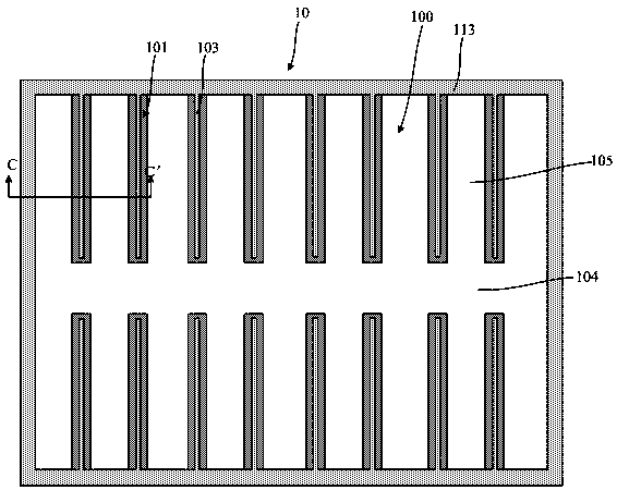
[0068] Such as Figure 5~Figure 6 As shown, among them, Figure 6 shown as Figure 5 The schematic diagram of the cross-sectional structure at CC' in the middle, this embodiment provides a high-power vertical cavity surface emitting laser with an integrated light emitting area, its basic structure is as in embodiment 1, wherein the vertical cavity surface emitting laser is a back emitting structure, The vertical cavity surface emitting laser includes: a P-type conductive lower reflector 211, the back of the P-type conductive lower reflector 211 has a lower electrode structure 107; an active layer 109 is located on the P-type conductive lower reflector 211 On; the N-type conductive upper reflector 208, located above the active layer 109, the N-type conductive upper reflector 208 has a current confinement layer 110, and the emission hole 10 is defined by the current confinement layer 110 The substrate 106 is located on the N-type conductive upper reflector 208, and the substra...
PUM
 Abstract
Description
Claims
Application Information


