Synaptic transistor, synaptic device, manufacturing method of synaptic transistor and synaptic device, and operation array

A technology of transistors and synapses, which is applied in the field of artificial intelligence and semiconductor device manufacturing, can solve the problems of difficult miniaturization and integration of devices, high power consumption, and low chip integration, so as to achieve miniaturization and integration, and high performance. consumption reduction effect

Active Publication Date: 2019-09-17
PEKING UNIV
View PDF4 Cites 13 Cited by
  • Summary
  • Abstract
  • Description
  • Claims
  • Application Information

AI Technical Summary

Problems solved by technology

However, in this way, simulating a synaptic behavior often requires multiple CMOS transistors, which makes the chip less integrated and consumes more power.
In addition, in some studies and applications, devices that use a transistor to simulate a synaptic behavior have also been proposed, such as memristor, phase-change RAM, spin RAM, iron Electric memory (ferroelectic RAM), these devices have the characteristics of simple structure and process, but the working speed of the device is not ideal
In addition, in some studies, it is also proposed to use MoO 3 , graphene, WSe 2 Three-terminal synaptic transistors are prepared with two-dimensional materials such as channel, but the gate dielectric still uses ionic liquid or solid electrolyte, and these devices are difficult to miniaturize and integrate

Method used


Image

  • Synaptic transistor, synaptic device, manufacturing method of synaptic transistor and synaptic device, and operation array
  • Synaptic transistor, synaptic device, manufacturing method of synaptic transistor and synaptic device, and operation array
  • Synaptic transistor, synaptic device, manufacturing method of synaptic transistor and synaptic device, and operation array

Examples


Embodiment Construction

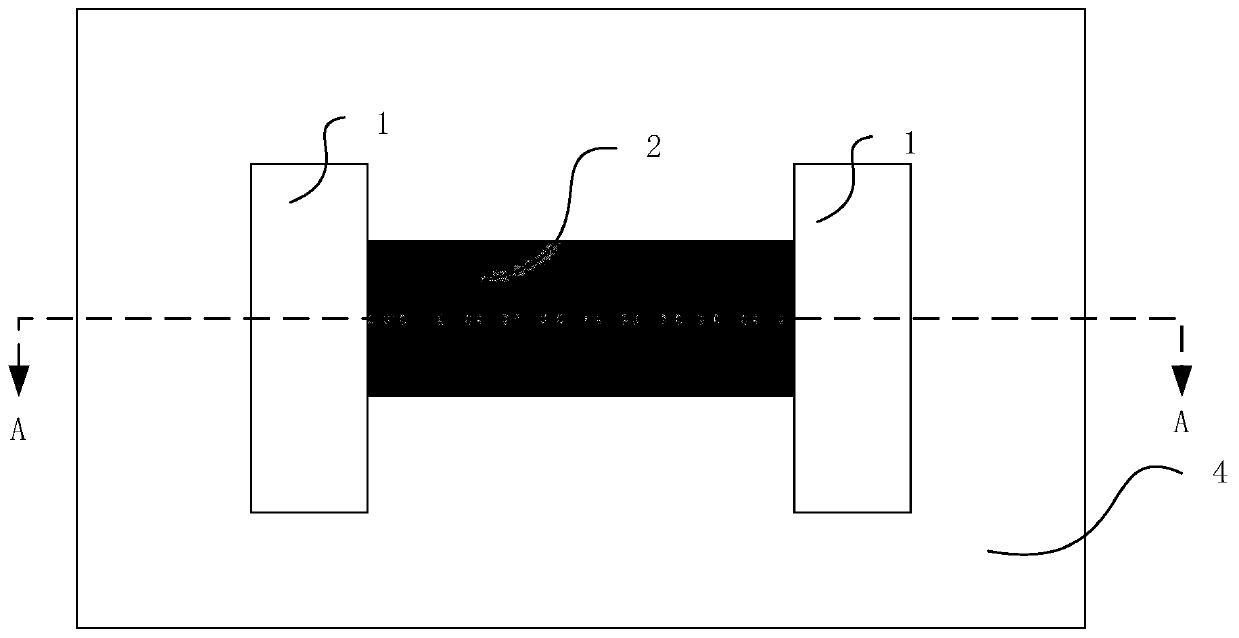
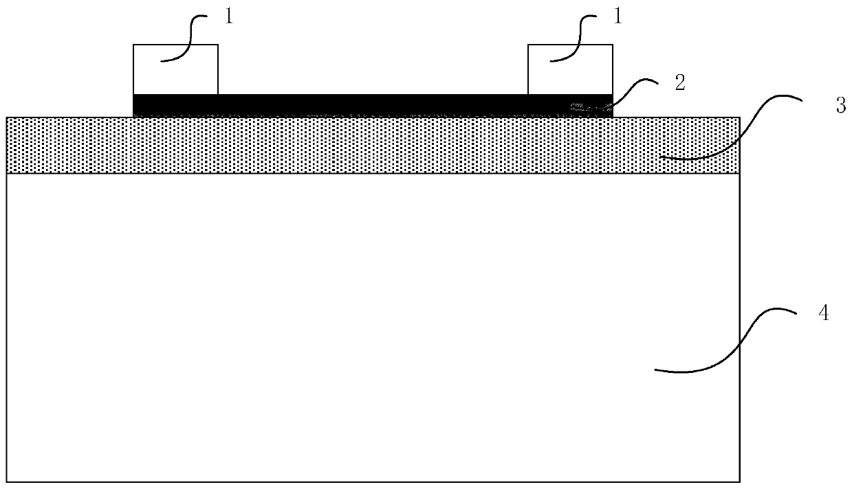
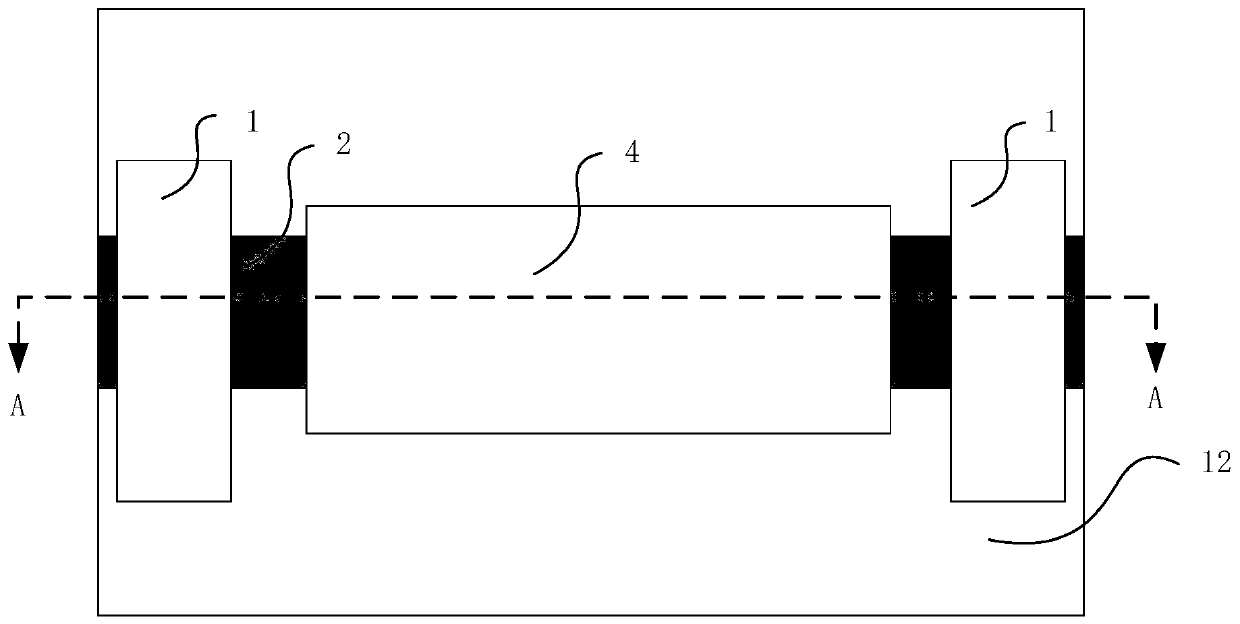
[0059] In order to make the above objects, features and advantages of the present invention more comprehensible, specific implementations of the present invention will be described in detail below in conjunction with the accompanying drawings.

[0060] In the following description, a lot of specific details are set forth in order to fully understand the present invention, but the present invention can also be implemented in other ways different from those described here, and those skilled in the art can do similar By extension, the present invention is therefore not limited to the specific examples disclosed below.

[0061] Secondly, the present invention is described in detail in combination with schematic diagrams. When describing the embodiments of the present invention in detail, for the convenience of explanation, the cross-sectional view showing the device structure will not be partially enlarged according to the general scale, and the schematic diagram is only an example...


PUM


Abstract

The invention provides a synaptic transistor, a synaptic device, a manufacturing method of the synaptic transistor and the synaptic device, and an operation array. The material of a channel layer of the device or the transistor is a semiconductor material with ferroelectric characteristics. By use of ferroelectric characteristics of a semiconductor material, a voltage is applied to the channel layer through a grid electrode or a source electrode and a drain electrode, so the ferroelectric domain in the channel layer is polarized and overturned and the conductivity of the channel layer is changed due to the change of the ferroelectric domain. Thus, the synaptic behaviors can be simulated through the change of the conductivity, so it is achieved that one synaptic behavior is simulated by using one transistor or device, the miniaturization and integration of the chip are facilitated, compatibility with the existing silicon-based technology is achieved, and the power consumption can be reduced.

Description

technical field [0001] The invention relates to the fields of artificial intelligence and semiconductor devices and manufacturing, in particular to a synaptic transistor, a device, a manufacturing method thereof, and an operation array. Background technique [0002] The artificial neural network is an algorithmic mathematical model that imitates the behavioral characteristics of the biological brain, especially the human brain, and synapses, and performs distributed parallel information processing. It can be widely used in the field of artificial intelligence. [0003] In the process of neuromorphic computing, a large number of matrix operations are involved. At present, the operation process is mainly realized by computer processors and memories. However, with the continuous increase of matrix scale, it poses a challenge to the computational efficiency of computer processors. At present, memory-computing integrated processing chips for neuromorphic computing have emerged a...

Claims


Application Information

Patent Timeline
Patent Type & Authority Applications(China)
IPC IPC(8): H01L29/06H01L29/41H01L21/336H01L29/78
CPCH01L29/0684H01L29/41H01L29/66409H01L29/78
Inventor 唐彬陈清廖建辉
Owner PEKING UNIV
Why Eureka
Try Eureka