Graphene-based LED epitaxial growth method

A technology of epitaxial growth and graphene, which is applied in the manufacture of semiconductor devices, electrical components, semiconductor/solid state devices, etc., can solve the problems of high chip grinding fragmentation rate, large warping of epitaxial wafers, and low product yield, so as to reduce epitaxy Effects of growth warping, improved crystal quality, and improved properties

Active Publication Date: 2021-12-07
XIANGNENG HUALEI OPTOELECTRONICS
View PDF9 Cites 0 Cited by
  • Summary
  • Abstract
  • Description
  • Claims
  • Application Information

AI Technical Summary

Problems solved by technology

In the current traditional epitaxial growth technology, the warpage of the epitaxial wafer is large, especially when the epitaxial crystal is grown on a large-sized sapphire substrate, the warpage is even greater, resulting in a high rate of grinding fragments and low product yield in the subsequent chip manufacturing process

Method used


Image

  • Graphene-based LED epitaxial growth method
  • Graphene-based LED epitaxial growth method
  • Graphene-based LED epitaxial growth method

Examples


Embodiment 1

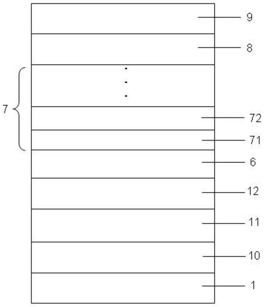
[0042] The invention uses PECVD to prepare graphene film on the sapphire substrate, and then uses MOCVD to grow high-brightness GaN-based LED epitaxial wafers. When growing high-brightness GaN-based LED epitaxial wafers, high-purity H 2 or high purity N 2 or high purity H 2 and high purity N 2 The mixed gas as the carrier gas, high-purity NH 3 As the N source, the metal-organic source trimethylgallium (TMGa), the metal-organic source triethylgallium (TEGa) is used as the gallium source, the trimethylindium (TMIn) is used as the indium source, and the N-type dopant is silane (SiH 4 ), trimethylaluminum (TMAl) as the aluminum source, and the P-type dopant as magnesium dicene (CP 2 Mg), the substrate is (0001) plane sapphire. The invention solves the problem of heterogeneous epitaxial growth of defects induced by lattice mismatch existing in the LED epitaxial growth in the prior art. The high-purity gas described in the present invention has a purity value of 99.999%, and t...

Embodiment 2

[0056] A conventional LED epitaxial growth method is provided below as a comparative example of the present invention.

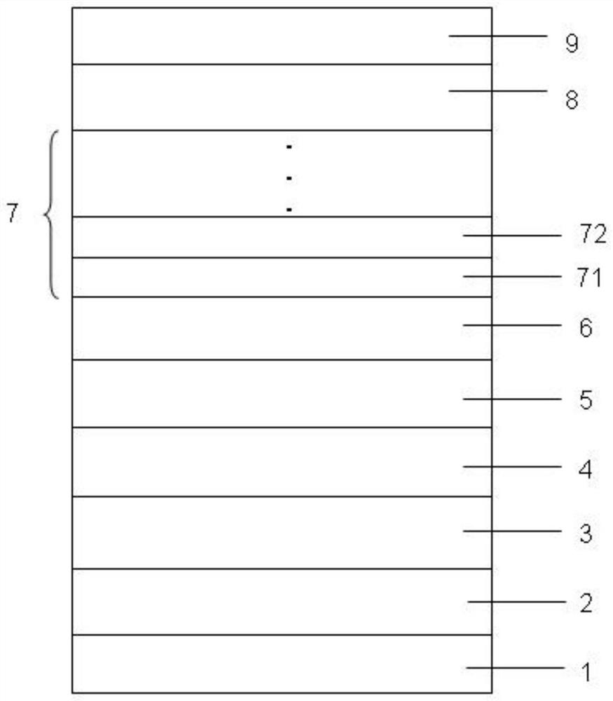
[0057] like figure 2 As shown, the conventional LED epitaxial growth method includes the following steps:

[0058] Step 1, processing sapphire substrate 1: Into the reaction chamber of the metal organic chemical vapor deposition system with the substrate placed, H at 900°C-1100°C 2 Under the atmosphere, feed 50L / min-100L / min of H 2 , keep the reaction chamber pressure at 100mbar-200mbar, and process the sapphire substrate for 5min-10min.

[0059] Step 2, grow GaN low-temperature buffer layer 10: cool down to 500°C-600°C, keep the reaction chamber pressure at 300mbar-600mbar, and feed NH with a flow rate of 40L / min-60L / min 3 , 50sccm-100sccm TMGa and 50L / min-90L / min H 2 , growing a GaN low-temperature buffer layer 10 with a thickness of 30nm-60nm on a sapphire substrate.

[0060] Step 3, grow 3D GaN layer 11: raise the temperature to 850°C-1000°C, keep ...


PUM

PropertyMeasurementUnit
thicknessaaaaaaaaaa

Abstract

This application discloses a graphene-based LED epitaxial growth method, which sequentially includes growing a high-temperature graded graphene layer, an n-type heavily doped AlN layer, a low-temperature graded graphene layer, and an n-type lightly doped AlN layer on a sapphire substrate. 1. Si-doped N-type GaN layer, periodically growing MQW active layer, P-type AlGaN layer, and Mg-doped P-type GaN layer, cooling down. The method of the present invention can reduce the warping of LED epitaxial wafers, improve the quality of epitaxial crystals, and improve the LED performance by adopting high-temperature gradient graphene layers, n-type heavily doped AlN layers, low-temperature gradient graphene layers, and n-type lightly doped AlN layers Photoelectric properties.

Description

technical field [0001] The present application relates to the technical field of LED epitaxial growth, in particular, to a graphene-based LED epitaxial growth method. Background technique [0002] LED (Light Emitting Diode, light-emitting diode) is a kind of solid-state lighting, which has the characteristics of small size, low power consumption, long service life, high brightness, environmental protection and durability, and is widely recognized by consumers. Therefore, domestic production The scale of LED is also gradually expanding. [0003] Sapphire is the most common substrate material for industrial growth of GaN-based LEDs at this stage. In the current traditional epitaxial growth technology, the warpage of the epitaxial wafer is large, especially when the epitaxial crystal is grown on a large-sized sapphire substrate, the warpage is even greater, resulting in a high rate of grinding fragments in the subsequent chip manufacturing process and a low product yield. [...

Claims


Application Information

Patent Timeline
Patent Type & Authority Patents(China)
IPC IPC(8): H01L33/32H01L33/06H01L33/00H01L21/02
CPCH01L21/0242H01L21/02444H01L21/0254H01L21/0262H01L33/0066H01L33/0075H01L33/06H01L33/32
Inventor 徐平龚彬彬廖富达周佐华黄胜蓝
Owner XIANGNENG HUALEI OPTOELECTRONICS
Why Eureka
Try Eureka