High frequency signal transmitting/receiving equipment

A technology for receiving equipment and high-frequency signals, applied in electromagnetic transceivers, optical radiation measurement, parallel plate/lens feeding arrays, etc. , the effect of low control power

Active Publication Date: 2021-02-26
SAMSUNG ELECTRONICS CO LTD
View PDF10 Cites 0 Cited by
  • Summary
  • Abstract
  • Description
  • Claims
  • Application Information

AI Technical Summary

Problems solved by technology

[0004] 1) high losses encountered when using standard semiconductor technology, resulting in low energy efficiency;
[0005] 2) Off-the-shelf components and circuits with low parasitic characteristics are complex or large and have high cost
[0013] The disadvantage of this solution is that a large number of photoconductive pixels are required for the device to provide acceptable scanning characteristics

Method used


Image

  • High frequency signal transmitting/receiving equipment
  • High frequency signal transmitting/receiving equipment
  • High frequency signal transmitting/receiving equipment

Examples


Embodiment Construction

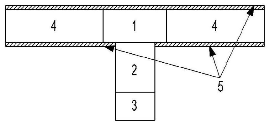
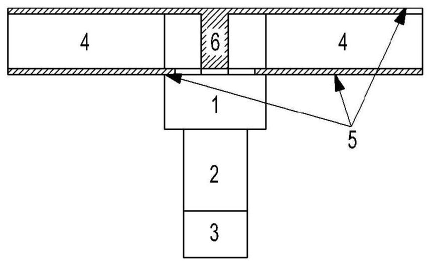
[0058] discussed below Figure 1 to Figure 18 The various embodiments used to describe the principles of the disclosure in this patent document are by way of illustration only and should not be construed in any way to limit the scope of the disclosure. Those skilled in the art will understand that the principles of the present disclosure may be implemented in any suitably arranged system or device.

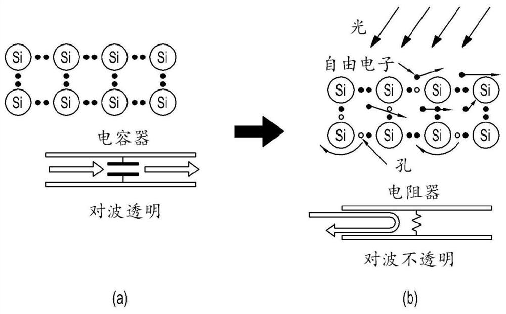
[0059] figure 1 a and 1b show the working principle of the light guiding element. As mentioned above, the present disclosure is based on switching between two states of a photoconductive element: a dielectric state with low intrinsic conductivity (off state) and a conductive state with relatively high conductivity under the action of light (connected state). status). Such as figure 1 As shown in a, in the off state, the structure of the photoconductive element is stable and non-conductive; the photoconductive element (PE) usually has capacitive properties and is transparent to...


PUM

PropertyMeasurementUnit
sizeaaaaaaaaaa
heightaaaaaaaaaa

Abstract

The present disclosure relates to radio engineering, and more particularly to high frequency (HF) signal transmitting / receiving devices based on photoconductive switching elements. The HF signal transmitting / receiving device comprises: a signal electrode with a matching element arranged along its edge; a ground electrode; a dielectric layer between the signal electrode and the ground electrode; photoconductive elements (PE), each electrically connected to the signal electrodes and ground electrodes and arranged in a grid; excitation signal feed points and load elements electrically connected to matching elements. The light guide elements each have an off state in the absence of a control light flux and an on state in the presence of a control light flux. The switched-on light-guiding element forms a reflection profile of the signal provided from the excitation signal feed point. The distance between adjacent light guiding elements is less than half the wavelength of the excitation signal.

Description

technical field [0001] Various exemplary embodiments of the present disclosure relate to a photoconductive element (PE) based high frequency signal transmitting / receiving device. Background technique [0002] The ever-increasing demands of users have stimulated the rapid development of mobile communication technology. Currently, 5G mmWave (millimeter wave) networks are being actively developed. 5G mmWave networks may require higher performance due to user experience requirements, including factors such as ease of connection with nearby devices and improved energy efficiency. mmWave technology encounters various fundamental challenges associated with the physics of antenna arrays, the construction of high-speed transceivers, and more. [0003] The fundamental challenges and limitations affecting current radio frequency (RF) signal transmitting / receiving devices (switches, phase shifters, antennas) operating at frequencies above 5 GHz are as follows: [0004] 1) high losses...

Claims


Application Information

Patent Timeline
Patent Type & Authority Patents(China)
IPC IPC(8): H01Q3/26G02B6/10
CPCG02B6/107G02B6/12002H01Q3/20H01Q3/24H01Q3/44H01Q9/30H01Q15/147H01Q19/138H01Q21/20H01Q25/00H01Q3/46H01Q15/04H01Q21/0031H01P1/15H01Q3/2676G02B6/10G01J1/04H01Q5/22H04B10/40H04Q11/0005H04Q2011/0035
Inventor M.N.马库林A.R.维伦斯基
Owner SAMSUNG ELECTRONICS CO LTD
Why Eureka
Try Eureka