OLED (Organic Light Emitting Diode) display substrate, manufacturing method thereof and display device

A technology for display substrates and manufacturing methods, which is applied in the fields of final product manufacturing, sustainable manufacturing/processing, semiconductor/solid-state device manufacturing, etc., and can solve the problems of reduced life of display panels, and achieve the effects of prolonging life and slowing down erosion

Inactive Publication Date: 2019-09-20
BOE TECH GRP CO LTD +1
View PDF3 Cites 6 Cited by
  • Summary
  • Abstract
  • Description
  • Claims
  • Application Information

AI Technical Summary

Problems solved by technology

When forming the pixel definition layer, a certain amount of material remains on both sides of the bulge, and the remaining material extends to the edge of the substrate, so that after covering the encapsulation layer, water and oxygen can flow along the remaining material to the OLED display substrate. Internal erosion, which reduces the life of the display panel

Method used


Image

  • OLED (Organic Light Emitting Diode) display substrate, manufacturing method thereof and display device
  • OLED (Organic Light Emitting Diode) display substrate, manufacturing method thereof and display device
  • OLED (Organic Light Emitting Diode) display substrate, manufacturing method thereof and display device

Examples


Embodiment Construction

[0039] In order to make the object, technical solution and advantages of the present invention clearer, the implementation manner of the present invention will be further described in detail below in conjunction with the accompanying drawings.

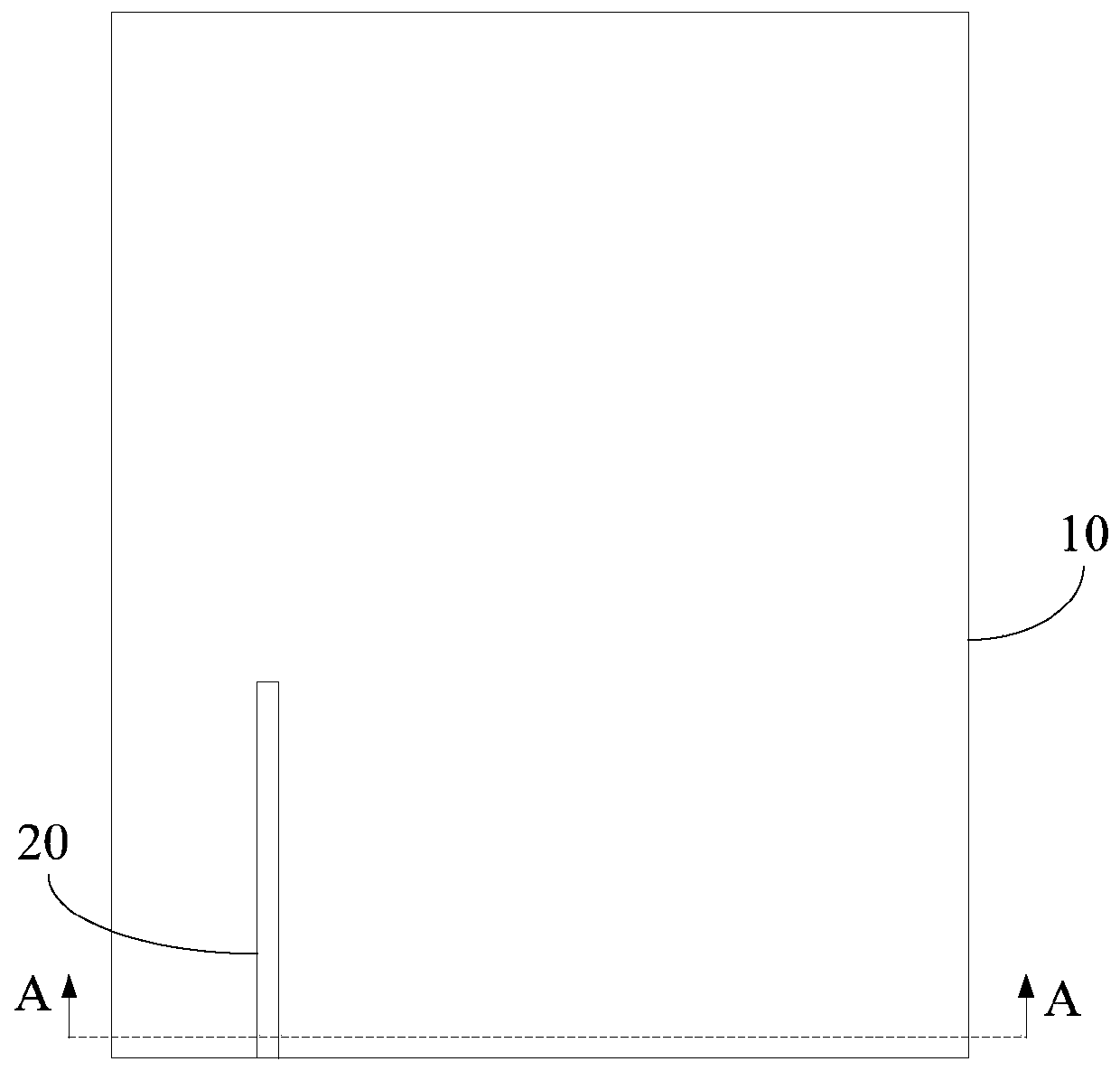
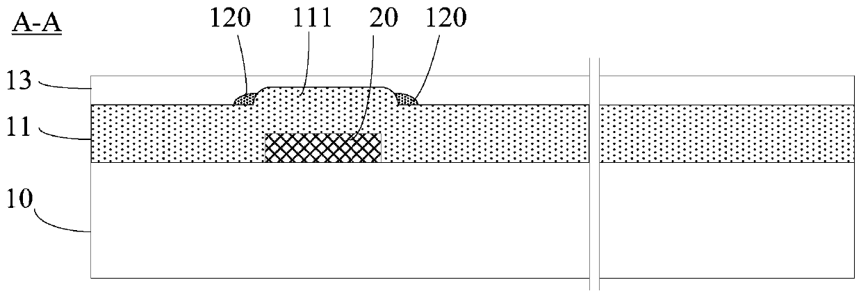
[0040] figure 1 It is a schematic diagram of a partial structure of an OLED display substrate. Such as figure 1 As shown, the OLED display substrate includes an insulating base 10 and a signal line 20 . One end of the signal line 20 extends to the edge of the insulating base 10, that is, one end of the signal line 20 is flush with the edge of the insulating base 10, which is for the convenience of connecting with other electrical structures, such as FPC (Flexible Printed Circuit Board, flexible circuit board) connect. figure 2 yes figure 1 A-A sectional view in . Such as figure 2 As shown, the OLED display substrate further includes a PLN (Planarization layer, planarization layer) 11 , a pixel definition layer (not shown in the...


PUM


Abstract

The invention discloses an OLED (Organic Light Emitting Diode) display substrate, a manufacturing method thereof and a display panel, and relates to the field of display devices. The OLED display substrate comprises an insulating substrate and a signal line, wherein one surface of the insulating substrate is provided with a groove, and the grooves extends from the edge of the insulating substrate to the middle of the insulating substrate; and the signal line is located on the surface, at least one segment of the signal line is located in the groove and extends to the edge of the insulating substrate along the groove. When the signal line is set, at least one segment of the signal line is enabled to be located in the groove, and the segment extends to the edge of the insulating substrate along the groove. Therefore, when a flattening layer is formed in the subsequent, the height of a bulge formed on the flattening layer can be reduced or the bulge can be eliminated because the signal line sinks into the groove, and the material residue formed at two sides of the bulge can be reduced or avoided when a pixel limiting layer is formed, thereby being capable of slowing down the erosion of water and oxygen into the OLED display substrate, and prolonging the life of the display panel.

Description

technical field [0001] The invention relates to the field of display devices, in particular to an OLED display substrate, a manufacturing method thereof, and a display device. Background technique [0002] Currently common display devices include passive light emitting display devices (such as liquid crystal display devices) and active light emitting display devices (such as OLED (Organic Light Emitting Diode, organic light emitting diode) display devices). Compared with the passive light-emitting display device, it has the advantages of smaller thickness, low power consumption, fast response speed, etc., so the active light-emitting display device has greater market competitiveness. [0003] The OLED display panel includes a boxed OLED display substrate and a cover plate. The OLED display substrate includes a substrate, a circuit layer on the substrate, a planarization layer, a pixel definition layer and a plurality of OLED light-emitting units. The OLED light-emitting unit...

Claims


Application Information

Patent Timeline
Patent Type & Authority Applications(China)
IPC IPC(8): H01L27/32H01L51/00H01L21/77
CPCH10K59/131H10K77/10H10K59/1201Y02P80/30Y02E10/549Y02P70/50
Inventor 于汇洋杨玉清张祎杨赵广洲程旭辉
Owner BOE TECH GRP CO LTD
Why Eureka
Try Eureka