Display mother board, preparation method thereof and electroluminescence display panels

A display panel and display substrate technology, applied in the direction of circuits, electrical components, electrical solid devices, etc., can solve the problems affecting the production yield of OLED display products, cutting damage, affecting cutting, etc., to achieve the effect of ensuring the production yield

Active Publication Date: 2019-09-27
BOE TECH GRP CO LTD +1
View PDF5 Cites 3 Cited by
  • Summary
  • Abstract
  • Description
  • Claims
  • Application Information

AI Technical Summary

Problems solved by technology

However, due to the adhesiveness of UV glue, its texture is relatively soft. In the process of vacuum bonding the cover glass and the back glass into the atmospheric pressure, such as image 3 As shown, the atmospheric pressure makes the UV glue 1 flow from the edge area along the inside of the glass to form a puncture shape 5, and the UV glue 1 exists in the area corresponding to the cutting line 3, which affects the subsequent cutting and causes the panel to be damaged
[0004] In summary, the packaging process of OLED display products in the prior art is prone to UV glue puncture, which affects the subsequent cutting process, causes cutting damage, and affects the production yield of OLED display products.

Method used


Image

  • Display mother board, preparation method thereof and electroluminescence display panels
  • Display mother board, preparation method thereof and electroluminescence display panels
  • Display mother board, preparation method thereof and electroluminescence display panels

Examples


Embodiment Construction

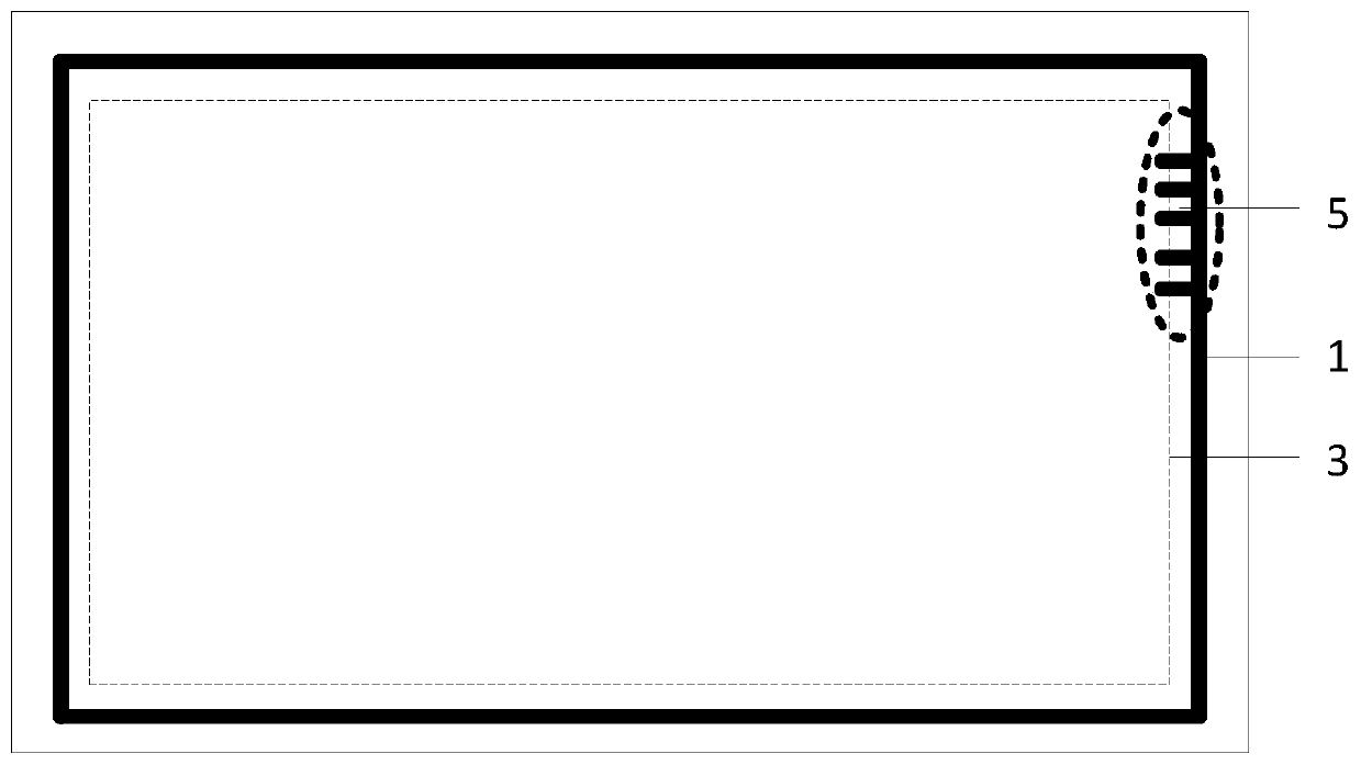
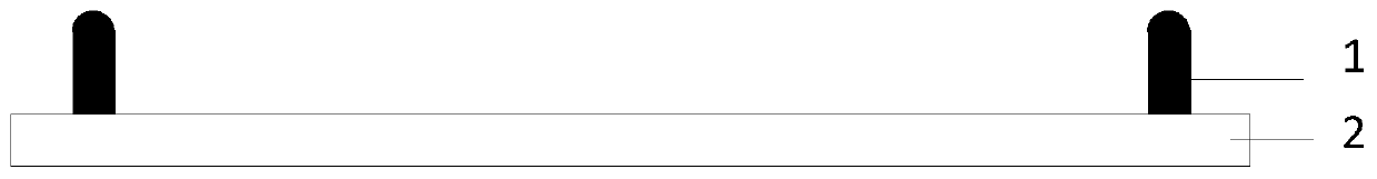
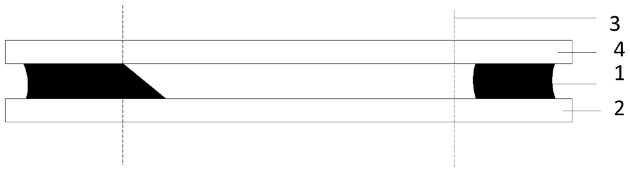
[0036] The embodiment of the present application provides a display motherboard provided in the embodiment of the present application, such as Figure 4 , Figure 5 As shown, among them, Figure 5 for Figure 4 In the cross-sectional view along AA', the display motherboard includes: a display substrate 6 and a cover plate 7 arranged oppositely; the display motherboard is divided into a display panel area 8 and a peripheral area 9 surrounding the display panel area 8; The display panel area 8 includes a plurality of electroluminescent display panels 14; the peripheral area 9 includes: a cutting area 10 and a packaging area 11 surrounding the cutting area 10; the packaging area 11 includes: sealing the display substrate 6 and the cover plate 7 and the sealant 12 surrounding the cutting area 10 , and the sealant blocking structure 13 located on the side of the sealant 12 facing the cutting area 10 .

[0037] In the display motherboard provided in the embodiment of the present ...


PUM


Abstract

The invention discloses a display mother board, a preparation method thereof and electroluminescence display panels, so as to prevent a sealant from flowing to a cutting area and ensure the display product preparation yield. The display mother board provided by the embodiment of the invention comprises a display substrate and a cover plate which are arranged oppositely. The display mother board is divided to a display panel area and a peripheral area surrounding the display panel area; the display panel area comprises multiple electroluminescence display panels; the peripheral area comprises a cutting area and a packaging area surrounding the cutting area; and the packaging area comprises the sealant sealing the display substrate and the cover plate and surrounding the cutting area and a sealant blocking structure located at one side, facing the cutting area, of the sealant.

Description

technical field [0001] The present application relates to the field of display technology, in particular to a display motherboard, a preparation method thereof, and an electroluminescence display panel. Background technique [0002] Organic Light Emitting Diode (OLED) display devices have self-illumination, low driving voltage, high luminous efficiency, short response time, high definition and contrast, viewing angle of nearly 180°, wide operating temperature range, and can realize flexible display and With many advantages such as large-area full-color display, it is recognized by the industry as a display device with the most potential for development. [0003] When making OLED display products, encapsulation process is required. One of the encapsulation methods is: apply glass glue (Frit glue) on the cover glass and attach it to the back glass, but the Frit glue will be textured after curing and before the laser process. Hard and non-adhesive to the backplane glass; there...

Claims


Application Information

Patent Timeline
Patent Type & Authority Applications(China)
IPC IPC(8): H01L27/32H01L51/52
CPCH10K59/10H10K50/84H10K50/8426
Inventor 徐东王强张瑞卿金文强
Owner BOE TECH GRP CO LTD
Why Eureka
Try Eureka