Etching method of semiconductor device and three-dimensional memory

A semiconductor and memory technology, applied in the field of semiconductor devices and their manufacturing, can solve the problems that the spacing cannot be further reduced, the device yield rate is reduced, and the layout of the three-dimensional memory array area is hindered, so as to improve the yield rate and work stability, and avoid offset Effect

Active Publication Date: 2019-10-18
YANGTZE MEMORY TECH CO LTD
View PDF3 Cites 5 Cited by
  • Summary
  • Abstract
  • Description
  • Claims
  • Application Information

AI Technical Summary

Problems solved by technology

[0004] However, the researchers found that in the process of forming GLS by dry etching process, the etching often cannot be performed along the direction vertical to the semiconductor substrate as expected, but tends to be inclined towards the CH direction; especially in the 90-layer In the above 3D NAND memory structure, the tilt phe

Method used


Image

  • Etching method of semiconductor device and three-dimensional memory
  • Etching method of semiconductor device and three-dimensional memory
  • Etching method of semiconductor device and three-dimensional memory

Examples


Embodiment 1

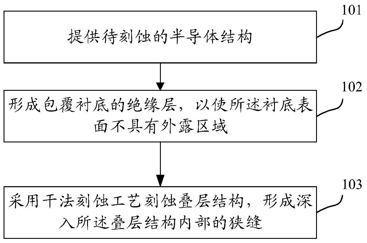
[0047] This embodiment provides an etching method for a semiconductor device; for details, please refer to the attached figure 2 . As shown, the method includes the following steps:

[0048] Step 101, provide a semiconductor structure to be etched, the semiconductor structure at least includes a semiconductor substrate, a stacked structure on the semiconductor substrate, and a first conductive column inside the stacked structure, the first The conductive pillar is electrically connected to the semiconductor substrate;

[0049] Step 102, forming an insulating layer covering the semiconductor substrate, so that the surface of the semiconductor substrate has no exposed area;

[0050] Step 103: Etching the stacked structure by using a dry etching process to form a slit deep inside the stacked structure.

[0051] It should be understood that the technical solution of the present invention is not limited to solving the offset problem generated when etching GLS in a three-dimensi...

Embodiment 2

[0073] This embodiment provides a method for manufacturing a three-dimensional memory, including the semiconductor device etching method described in any of the foregoing embodiments; for details, please refer to the attached Figure 5 . As shown, the method includes the following steps:

[0074] Step 201, providing a semiconductor substrate, and forming a stacked structure on the semiconductor substrate;

[0075] Step 202: Etching the stacked structure to form a channel via hole penetrating through the stacked structure, forming a channel structure inside the channel via hole, the channel structure at least includes a channel layer, the The channel layer is electrically connected to the semiconductor substrate;

[0076] Step 203, forming an insulating layer covering the semiconductor substrate, so that there is no exposed area on the surface of the semiconductor substrate;

[0077] Step 204 , etching the stacked structure by using a dry etching process to form a gate slit ...

Embodiment 3

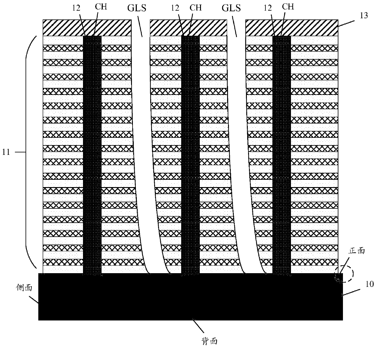
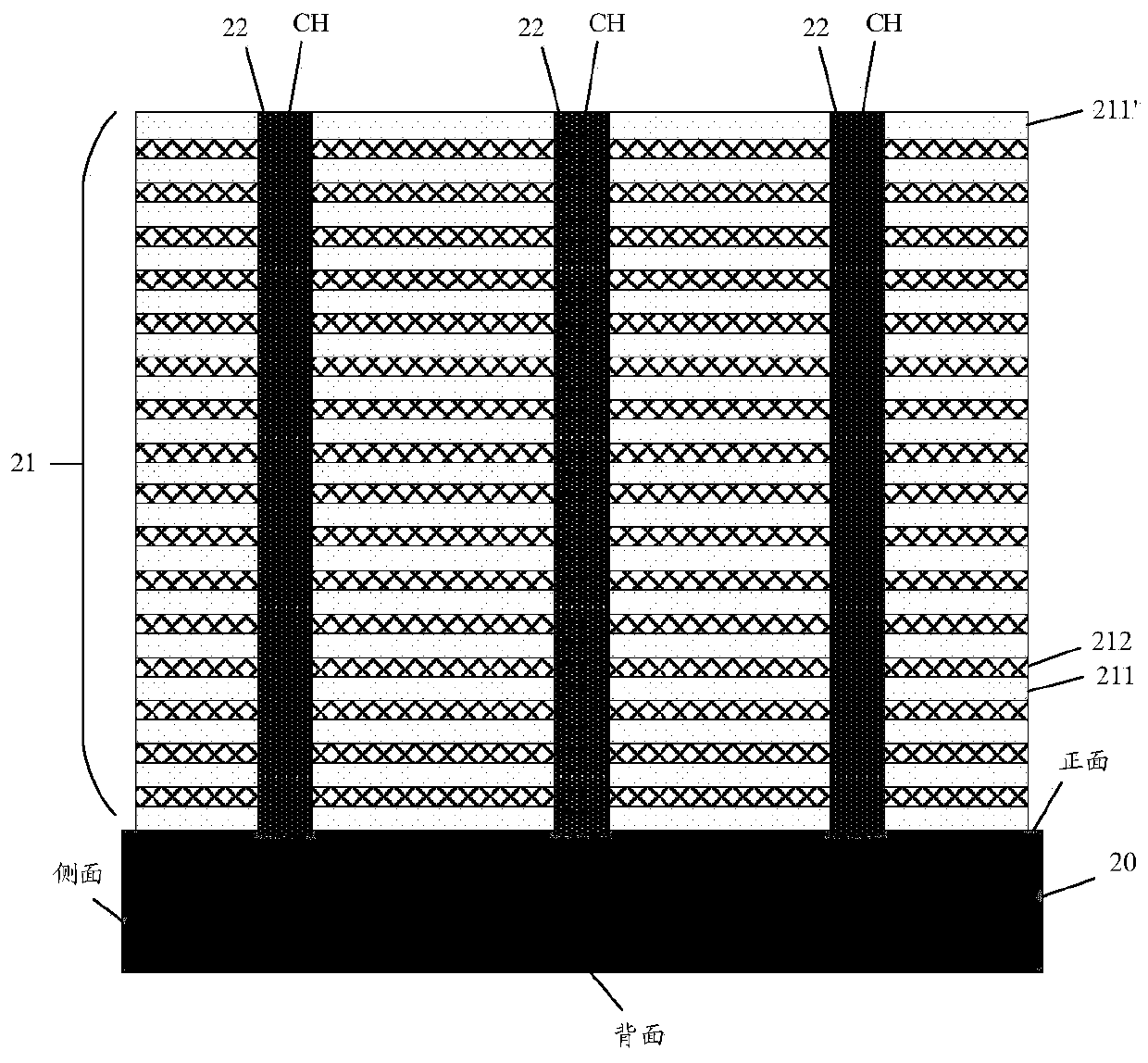
[0080] This embodiment provides a three-dimensional memory, for details, please refer to the attached Figure 3d . As shown in the figure, the three-dimensional memory includes: a semiconductor substrate 20, a stacked structure 21 located on the semiconductor substrate 20, and a channel hole CH penetrating through the stacked structure 21; the inside of the CH is provided with channel layer 22, the channel layer 22 is electrically connected to the semiconductor substrate 20; the three-dimensional memory also includes an insulating layer 24 covering the semiconductor substrate 20, so that the surface of the semiconductor substrate 20 is not have exposed areas.

[0081] In a specific embodiment, the laminated structure 21 includes a plurality of alternately arranged first material layers 211 and second material layers 212 . The first material layer 211 is a dielectric layer; the second material layer 212 is a gate layer or a dummy gate layer.

[0082] In a specific embodiment...


PUM

PropertyMeasurementUnit
Thicknessaaaaaaaaaa
Thicknessaaaaaaaaaa

Abstract

The invention discloses an etching method of a semiconductor device and a three-dimensional memory. The etching method comprises the steps of providing a to-be-etched semiconductor structure, whereinthe semiconductor structure comprises at least one semiconductor substrate, a laminated structure located on the semiconductor substrate and first conductive columns located in the laminated structure; and the first conductive columns are conductively connected with the semiconductor substrate; forming an insulating layer coating the semiconductor substrate to avoid an exposed area on the surfaceof the semiconductor substrate; and etching the laminated structure by adopting a dry etching process and forming slits penetrating into the laminated structure, thereby ensuring that the dry etchingprocess is carried out in the expected direction and improving the yield and the working stability of the device.

Description

technical field [0001] The invention relates to the field of semiconductor devices and their manufacture, in particular to an etching method for semiconductor devices and a three-dimensional memory. Background technique [0002] Memory is a memory device used to save information in modern information technology. With the continuous improvement of the demand for integration and data storage density of various electronic devices, it is becoming more and more difficult for ordinary two-dimensional memory devices to meet the requirements. In this case, three-dimensional (3D) memory comes into being. [0003] At present, in the preparation process of a three-dimensional memory, generally a semiconductor substrate is provided first and a stacked structure is formed on the semiconductor substrate; then, the stacked structure is etched by a dry etching process to form a layer exposing the semiconductor substrate. Channel hole (Chanel Hole, CH), and a channel structure is formed in...

Claims


Application Information

Patent Timeline
IPC IPC(8): H01L21/033H01L27/11578
CPCH01L21/0337H10B43/20
Inventor 许波杨川谢柳群殷姿
Owner YANGTZE MEMORY TECH CO LTD
Why Eureka
Try Eureka