

Method for manufacturing semiconductor three-dimensional Hall sensor suitable for high-temperature working environment
A Hall sensor, working environment technology, applied in the direction of instruments, single equipment manufacturing, measuring devices, etc., can solve the problems of the multi-dimensional Hall sensor system is bulky, complex chip layout, unable to work normally, etc., to improve the measurement sensitivity, volume Small, good chemical stability effect
- Summary
- Abstract
- Description
- Claims
- Application Information
AI Technical Summary
Problems solved by technology
Method used
Image

Examples
Embodiment 1
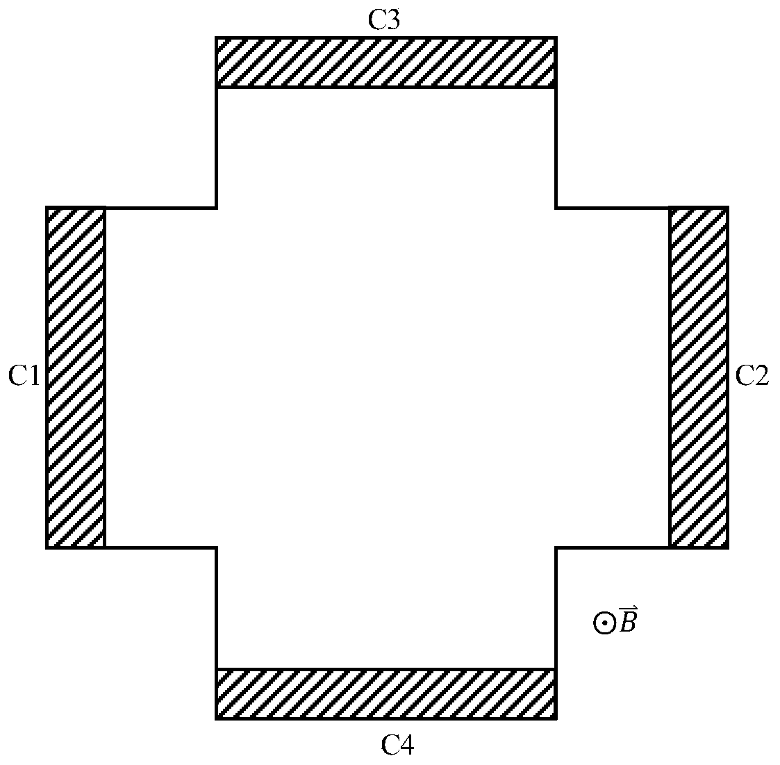
[0045] Such as Figure 4 As shown, wide bandgap semiconductor materials such as SiC or GaN are used, and 5 main electrodes and 8 Hall sensing electrodes are designed and fabricated on the surface of the material, and the metal / semiconductor contact type is ohmic contact. Among them, the 5 main electrodes are 1 central current inflow electrode (B) and 4 current outflow electrodes (B X1 , B X2 , B Z1 and B Z2 ), the 8 Hall sensing electrodes are X 1 ~X 4 and Z 1 ~ Z 4 , where two pairs of Hall sensing electrodes X 1 、X 2 and x 3 、X 4 Measure two magnetic field components in space (X and Z directions), and the remaining four Hall sensing electrodes Z 1 ~ Z 4 Measure the third magnetic field component (Y direction).
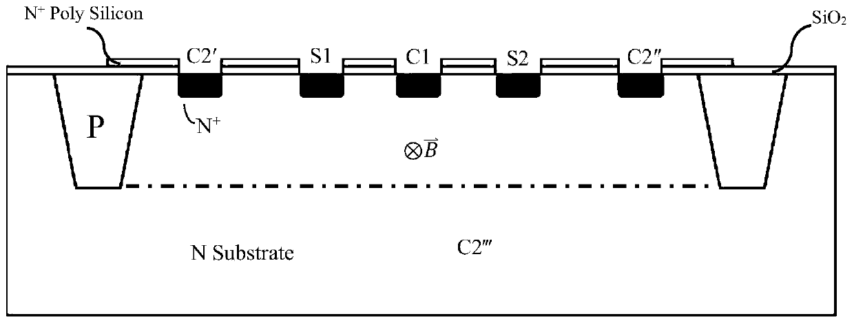
[0046] Using insulating layers ①, ②, ③ and ④ embedded between the Hall sensing electrodes, the insulating layer material can be SiO 2 、Si 3 N 4 、Al 2 o 3 etc., using this technology can effectively guide the sensing current direction while significa...
Embodiment 2
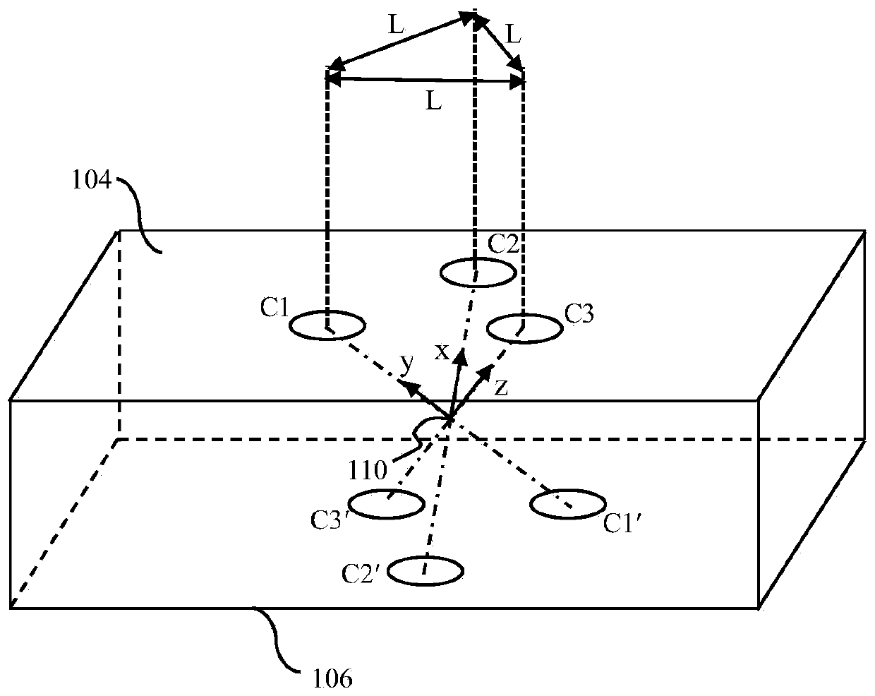
[0066] In this embodiment, the intrinsic GaN material is used, and the background carrier concentration of the material is 5×10 15 cm -3 , the insulating layer material used is Si 3 N 4 . The three main electrodes B and B of the device chip X1 , B X2 The size is 40μm×10μm, and the remaining two main electrodes B Z1 , B Z2 The size is 10μm×10μm, Hall sensing electrode Z 1 ~ Z 4 、X 1 ~X 4 The size is 10μm×10μm, the size of each embedded isolation insulating layer is 40μm×60μm, and the Hall sensing electrode X 1 、X 2 The distance between the center and the center of the center main electrode B is 45 μm, and the Hall sensing electrode X 3 、X 4 The distance between the center and the center of the center main electrode B is 30 μm, and the main electrode B Z1 , B Z2 The distance between the center and the center of the center main electrode B is 75 μm, and the main electrode B X1 , B X2 The distance between the center and the center of the center main electrode B is...
Embodiment 3
[0074] As a separate embodiment or as a supplement to Embodiment 1, the central current flowing into the electrode B adopts a circular or rectangular shape; the current flowing out of the electrode B X1 , B X2 , B Z1 , B Z2 Rectangular shape is preferred for the eight Hall sensing electrodes, and circular shape can also be used.
PUM
 Abstract
Description
Claims
Application Information