Substrate stacked packaging structure and packaging method thereof

A packaging structure and substrate technology, applied in the direction of semiconductor/solid-state device components, semiconductor devices, electrical components, etc., can solve problems such as complex functions, and achieve the effects of increasing electrical connection methods, reducing package size, and protecting pads

Active Publication Date: 2020-12-25
上海彤程电子材料有限公司 +1
View PDF5 Cites 0 Cited by
  • Summary
  • Abstract
  • Description
  • Claims
  • Application Information

AI Technical Summary

Problems solved by technology

In this way, the integration level of integrated circuits is required to be higher and higher, and the functions are more and more complex.

Method used


Image

  • Substrate stacked packaging structure and packaging method thereof
  • Substrate stacked packaging structure and packaging method thereof
  • Substrate stacked packaging structure and packaging method thereof

Examples


Embodiment Construction

[0027] The object of the present invention is to provide a packaging structure and packaging method with simple packaging process, small thickness and high integration.

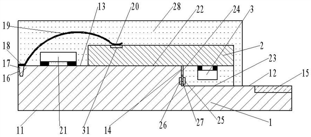
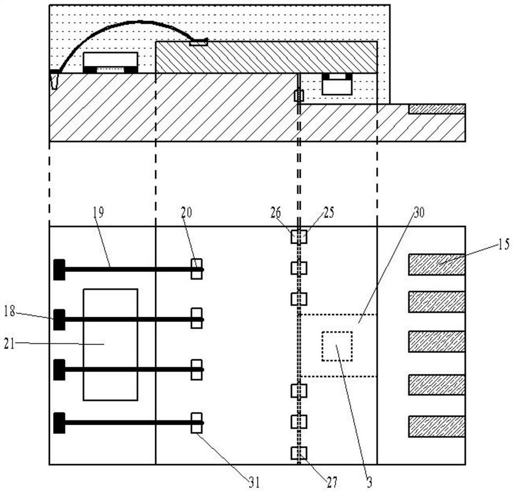
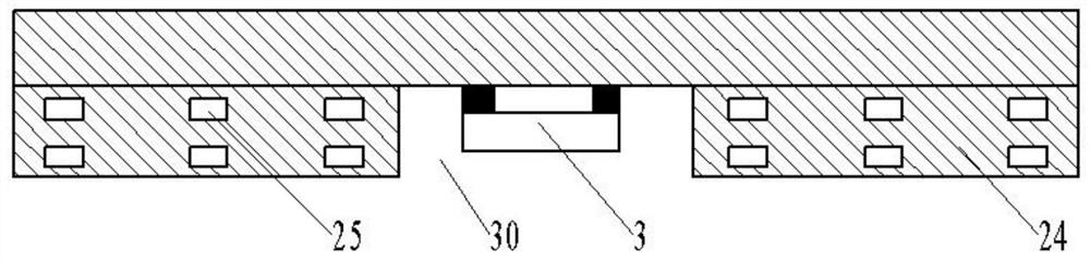
[0028] join Figure 1-4 , the through-hole substrate-on-substrate package structure of the present invention includes a first substrate 2 and a second substrate 1, the first substrate 2 is an additional substrate, and the second substrate 1 is a packaging substrate or a system board, both of which can make a PCB plate or ceramic substrate. Wherein the first substrate 2 includes a first bottom surface 22 and a second bottom surface 23, a first top surface opposite to the first and second bottom surfaces, and a first connecting surface 24 connecting the first and second bottom surfaces, The first bottom surface and the second bottom surface have a height difference, the first bottom surface 22, the second bottom surface 23 and the first connecting surface 24 form a first zigzag step, and the first connecting s...


PUM


Abstract

The invention provides a substrate superposition packaging structure and packaging method. The substrate superposition packaging structure comprises a first substrate and a second substrate, wherein the first substrate has a first Z-shaped step, and the second substrate is provided with a second Z-shaped step; the first Z-shaped step and the second Z-shaped step are matched in shape, a first bottom surface of the first substrate is in contact with a second top surface of the second substrate, a second bottom surface of the first substrate is in contact with a third top surface of the second substrate, and a first pad of the first substrate is electrically connected with a second pad of the second substrate through a conductive bonding layer.

Description

technical field [0001] The invention relates to the field of semiconductor integrated circuit packaging, belongs to the H01L23 / 00 classification number, and in particular relates to a substrate stacked packaging structure and a packaging method thereof. Background technique [0002] Integrated circuit packaging is advancing along with the development of integrated circuits. With the continuous development of various industries such as aerospace, aviation, machinery, light industry, and chemical industry, the whole machine is also changing in the direction of multi-function and miniaturization. In this way, the integration level of integrated circuits is required to be higher and higher, and the functions are more and more complex. Correspondingly, it is required that the packaging density of integrated circuits is increasing, the number of leads is increasing, the volume is getting smaller, the weight is getting lighter, and the replacement is getting faster and faster. The...

Claims


Application Information

Patent Timeline
Patent Type & Authority Patents(China)
IPC IPC(8): H01L23/13H01L23/488H01L21/50H01L21/60
CPCH01L21/50H01L23/13H01L23/488H01L24/81H01L2224/818H01L2224/16225H01L2224/48091H01L2924/00014
Inventor 秦玲
Owner 上海彤程电子材料有限公司
Why Eureka
Try Eureka