CC pin circuit of USB Type-C

A circuit and pin technology, which is applied in the field of CC pin circuit of USB Type-C, can solve the problems of inability to activate and realize CC connection, and achieve the effect of realizing high voltage protection and solving the problem of withstand voltage

Pending Publication Date: 2019-10-25
ZHUHAI ISMARTWARE TECH CO LTD
View PDF0 Cites 7 Cited by
  • Summary
  • Abstract
  • Description
  • Claims
  • Application Information

AI Technical Summary

Problems solved by technology

At this time, connecting to SRC or other DRP cannot form a pull-down path connected to the CC pin. When the Rp_SRC resistor Ⅴ of the Type-C interface at the other end appears, it will pull up the voltage of the CC pin Ⅳ to the power supply of the Type-C interface at the other end. VDDSRC, so the CC connection cannot be realized, and the Type-C interface at the other end will not output VBUS, resulting in the dead battery state being unable to be activated.
This situation is often unacceptable in practical applications

Method used


Image

  • CC pin circuit of USB Type-C
  • CC pin circuit of USB Type-C
  • CC pin circuit of USB Type-C

Examples


Embodiment Construction

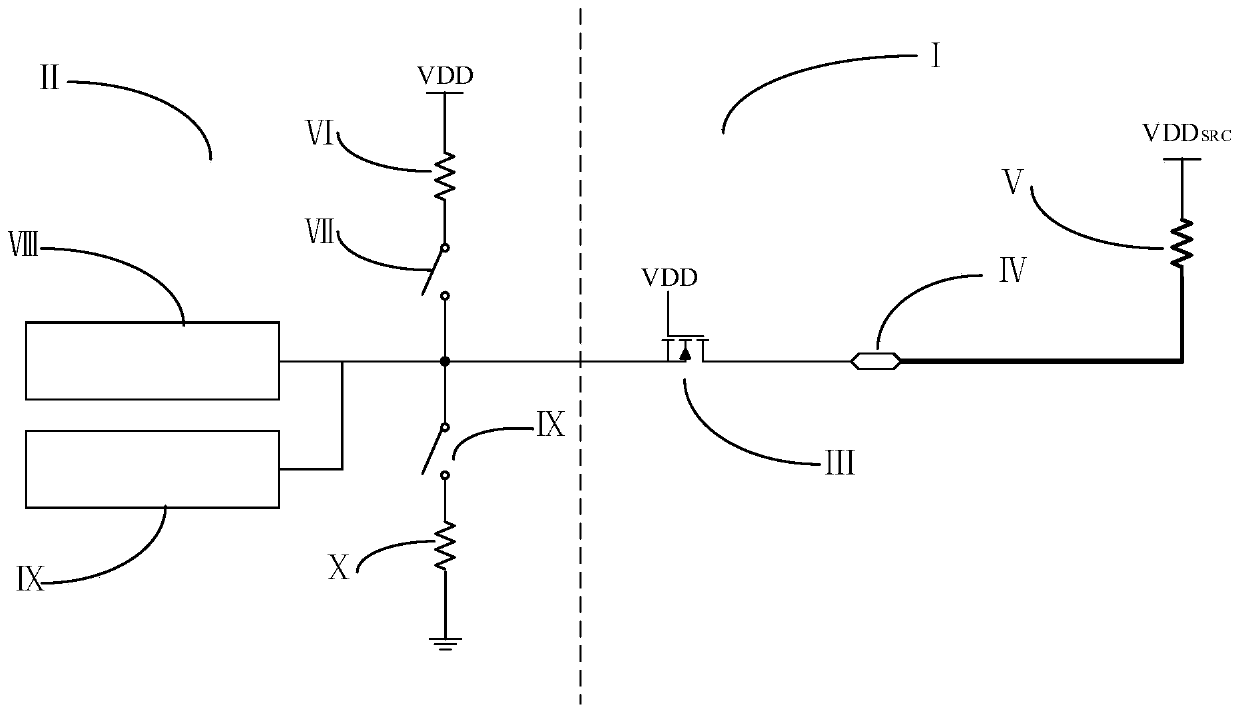
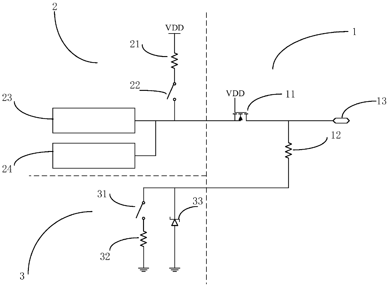
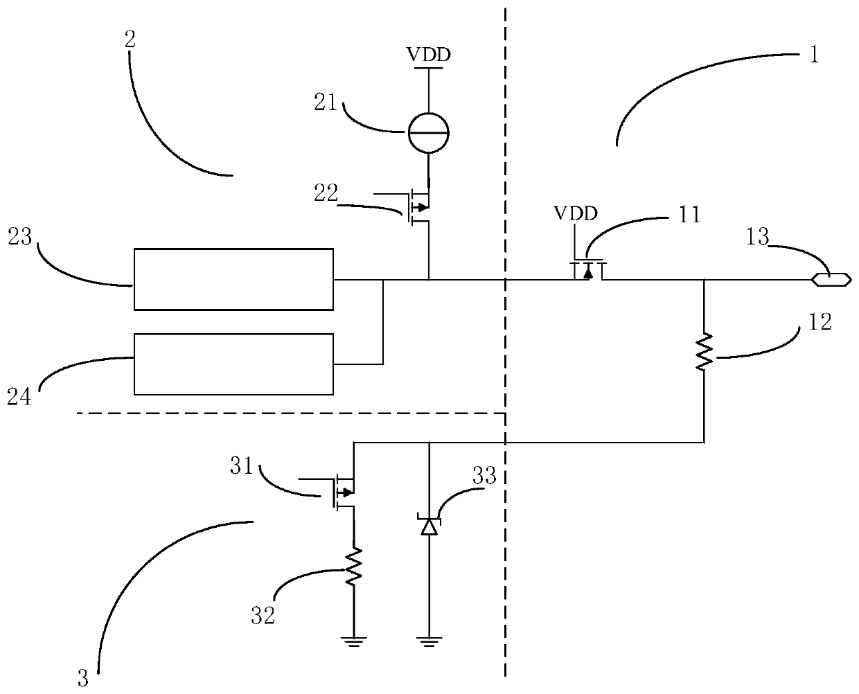
[0026] see figure 2 , figure 2 It is a schematic diagram of the CC pin circuit structure of USB Type-C in the present invention. The CC pin circuit includes a high-voltage NMOS11, a pull-up resistor circuit, a CC connection detection circuit 23, a PD communication circuit 24, a pull-down resistor circuit, and a voltage clamping circuit. The gate of the high-voltage NMOS11 is connected to the internal power supply VDD, and the pull-up resistor circuit, CC One end of the connection detection circuit 23 and the PD communication circuit 24 are both connected to the source of the high-voltage NMOS, the drain of the high-voltage NMOS11 is connected to the pull-down resistor circuit, and the drain of the high-voltage NMOS11 is connected to the first end of the CC pin, and the pull-down resistor circuit includes The first resistance circuit and the second resistance circuit, and the voltage clamping circuit are connected between the series node of the first resistance circuit and t...


PUM


Abstract

The invention provides a CC pin circuit of USB Type-C. In the Type-C interface circuit, a high-voltage NMOS is introduced for voltage isolation, and a first low-voltage region is generated. A pull-upresistor circuit, a CC connection detection circuit, a PD communication circuit and the like are placed in the first low-voltage region to realize high-voltage protection. The pull-down resistor circuit is directly connected to the CC pin, so that when the Type-C interface is in a Dead Battery state in a DRP or SNK mode, the CC connection can be normally realized by accessing the SRC or other DRPs(Data Redundancy Protocol). And a resistor in the pull-down resistor circuit is divided into a first resistor and a second resistor which are connected in series, and voltage clamping is performed ata middle series node to generate a second low-voltage region. And an enable control switch of the pull-down resistor circuit and the second resistor are placed in the second low-voltage region to realize high-voltage protection. The first resistor is placed in a high-voltage area and plays a role in current limiting when the voltage clamping circuit works. The withstand voltage design method andthe circuit structure can be applied to Type-of all modes. And in the C interface circuit, the voltage withstanding problem of the CC pin is solved.

Description

technical field [0001] The invention relates to the technical field of USB Type-C interface circuits, in particular to a CC pin circuit of USB Type-C. Background technique [0002] With the rapid development of electronic technology, portable electronic products represented by mobile phones, tablets and notebook computers have widely affected people's daily life. The new USB Type-C interface supports front and back insertion, which solves the worldwide problem of "USB can never be inserted correctly". In addition, compared with the traditional USB interface, the Type-C interface has the characteristics of lighter weight, thinner design, smaller size, and stronger expandable functionality, which is very suitable for application in portable electronic products. Since the Type-C interface came out, it has been widely popularized in just a few years. [0003] With the rise of USB fast charging technology, the voltage transmitted by VBUS in the USB interface is no longer a fixe...

Claims


Application Information

Patent Timeline
Patent Type & Authority Applications(China)
IPC IPC(8): H03K19/0175H03K19/003G06F13/40G06F13/42
CPCG06F13/4063G06F13/4282H03K19/00307H03K19/00315H03K19/017509
Inventor 梁源超李进邓琴
Owner ZHUHAI ISMARTWARE TECH CO LTD
Why Eureka
Try Eureka