
Operational amplifier compensation circuit applied to bidirectional open-drain output buffer

A technology of output buffer and compensation circuit, which is applied in the direction of logic circuit coupling/interface and logic circuit connection/interface arrangement using field effect transistors, which can solve the problem of increasing the output voltage switching range, increasing the loop stabilization time, reducing Issues such as transmission signal rate to reduce the possibility of overshoot and oscillation, improve stability and accuracy, and shorten response time

Active Publication Date: 2019-10-25
3PEAK INC
View PDF4 Cites 0 Cited by
  • Summary
  • Abstract
  • Description
  • Claims
  • Application Information

AI Technical Summary

Problems solved by technology

However, similar traditional compensation methods have brought many problems at the same time, either greatly increasing the stabilization time of the loop, seriously reducing the rate of transmission signals, or reducing the gain of the operational amplifier and increasing the output voltage. poor range and stability

Method used


Image

  • Operational amplifier compensation circuit applied to bidirectional open-drain output buffer
  • Operational amplifier compensation circuit applied to bidirectional open-drain output buffer
  • Operational amplifier compensation circuit applied to bidirectional open-drain output buffer

Examples


Embodiment Construction

[0012] The specific implementation of the present invention will be described in further detail below in conjunction with the accompanying drawings of the embodiments, so as to make the technical solution of the present invention easier to understand and grasp, so as to define the protection scope of the present invention more clearly.

[0013] The designer of the present invention aims at the design of the loop compensation in the bidirectional open-drain output buffer in the prior art. There are problems such as increasing the loop stabilization time, reducing the transmission signal rate and increasing the output voltage signal switching range, and the open-drain output performance cannot meet all requirements. A comprehensive analysis of the circuit structure was carried out for the many deficiencies needed. Combining its own experience and creative work, it is committed to seeking a breakthrough in the all-round optimization of the circuit performance, and innovatively prop...


PUM


Abstract

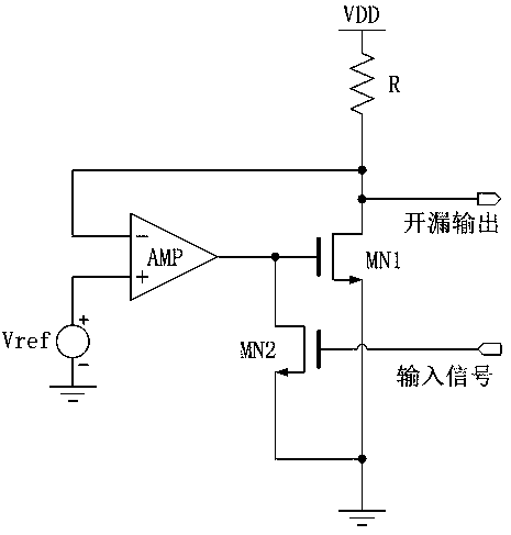
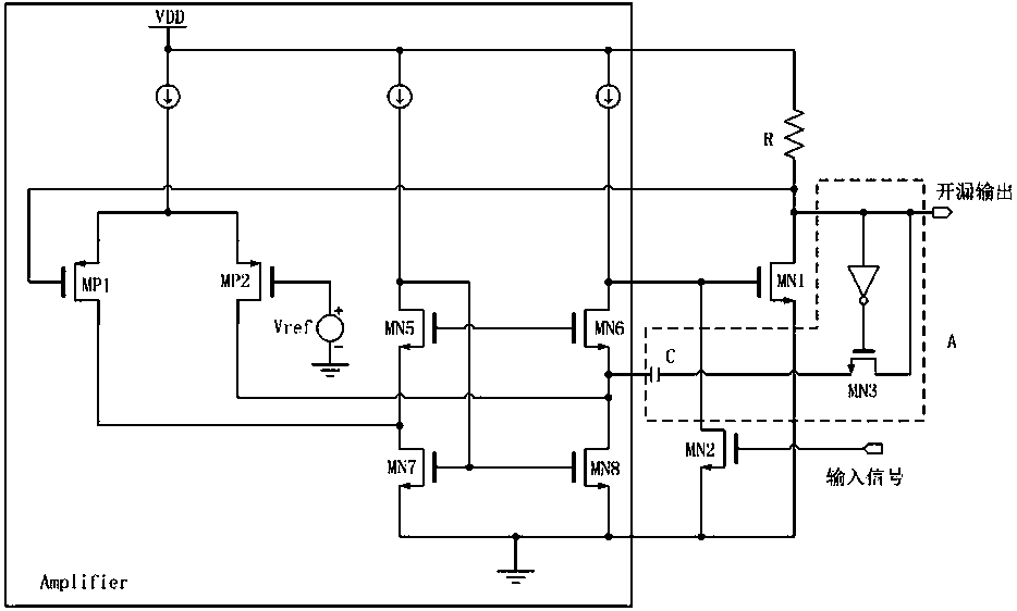
The invention discloses an operational amplifier compensation circuit applied to a bidirectional open-drain output buffer. The bidirectional open-drain output buffer is formed by connecting an amplifier AMP, a pull-up resistor R, an NMOS tube MN1 and an NMOS tube MN2, wherein the anode input end of the amplifier AMP is connected with a reference voltage Vref, the negative input end of the amplifier AMP is connected with one end of the pull-up resistor R and the drain electrode of the MN1 to form an open drain output end, the other end of the pull-up resistor R is connected with a voltage VDD,the output end of the amplifier AMP is connected with the grid electrode of the MN1 and the drain electrode of the MN2, the MN1 and the MN2 are in common source grounding, and the grid electrode of the MN2 receives input signals. The operational amplifier compensation circuit with the characteristic design is formed by connecting a compensation capacitor C, an NMOS tube MN3 and an inverter. One end of the phase inverter and the drain electrode of the MN3 are connected with the open drain output end, the other end of the phase inverter is connected with the grid electrode of the MN3, and the source electrode of the MN3 is connected into the drain electrode of the PMOS tube where the positive electrode input end of the amplifier AMP is located through the compensation capacitor C. The compensation circuit design has the advantages that the loop response time is shortened, and the stability and precision of the output voltage are improved.

Description

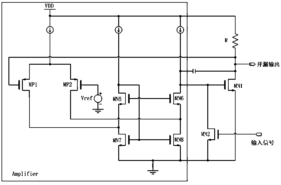
technical field [0001] The invention relates to an improved design of a bidirectional open-drain output buffer, in particular to an operational amplifier compensation circuit applied to the bidirectional open-drain output buffer and having high stability, precision and fast response rate. Background technique [0002] Bidirectional open-drain output buffers usually need to maintain the low level of the open-drain output in one direction at a fixed voltage to avoid a loop-locked state. Conventional circuits for this purpose usually rely on a pull-up resistor R and an amplifier AMP, as shown in 1 below. [0003] However, the input signal has instability such as overshoot and oscillation, so some compensation is required for the loop. like figure 2 A traditional compensation circuit design is shown, that is, a capacitor is connected between the open-drain output terminal and the output terminal of the amplifier. However, similar traditional compensation methods have brought ...

Claims


Application Information

Patent Timeline
Patent Type & Authority Applications(China)
IPC IPC(8): H03K19/0185
CPCH03K19/0185
Inventor 陶园林向飞翔
Owner 3PEAK INC
Learn More