
An automatic layout equipment for semiconductor patch welding

A patch welding and semiconductor technology, applied in electrical components, electrical components, etc., can solve the problems of tired work, high labor intensity, and high cost of robot patching, and achieve high positioning accuracy, continuous and automatic feeding, and small vibration effects.

Active Publication Date: 2020-04-28
台州市黄岩日隆模具厂(普通合伙)
View PDF9 Cites 0 Cited by
  • Summary
  • Abstract
  • Description
  • Claims
  • Application Information

AI Technical Summary

Problems solved by technology

[0002] The welding of semiconductor chips has always been a very delicate work. Whether it is manual placement or machine placement, it requires very high operational accuracy and stability. However, most of the existing manual placement, although experienced workers It can be placed very well, but the work is tiring
The labor intensity is very high; the cost of robot placement is very high, and it must be applied by medium and large enterprises

Method used


Image

  • An automatic layout equipment for semiconductor patch welding
  • An automatic layout equipment for semiconductor patch welding
  • An automatic layout equipment for semiconductor patch welding

Examples


Embodiment

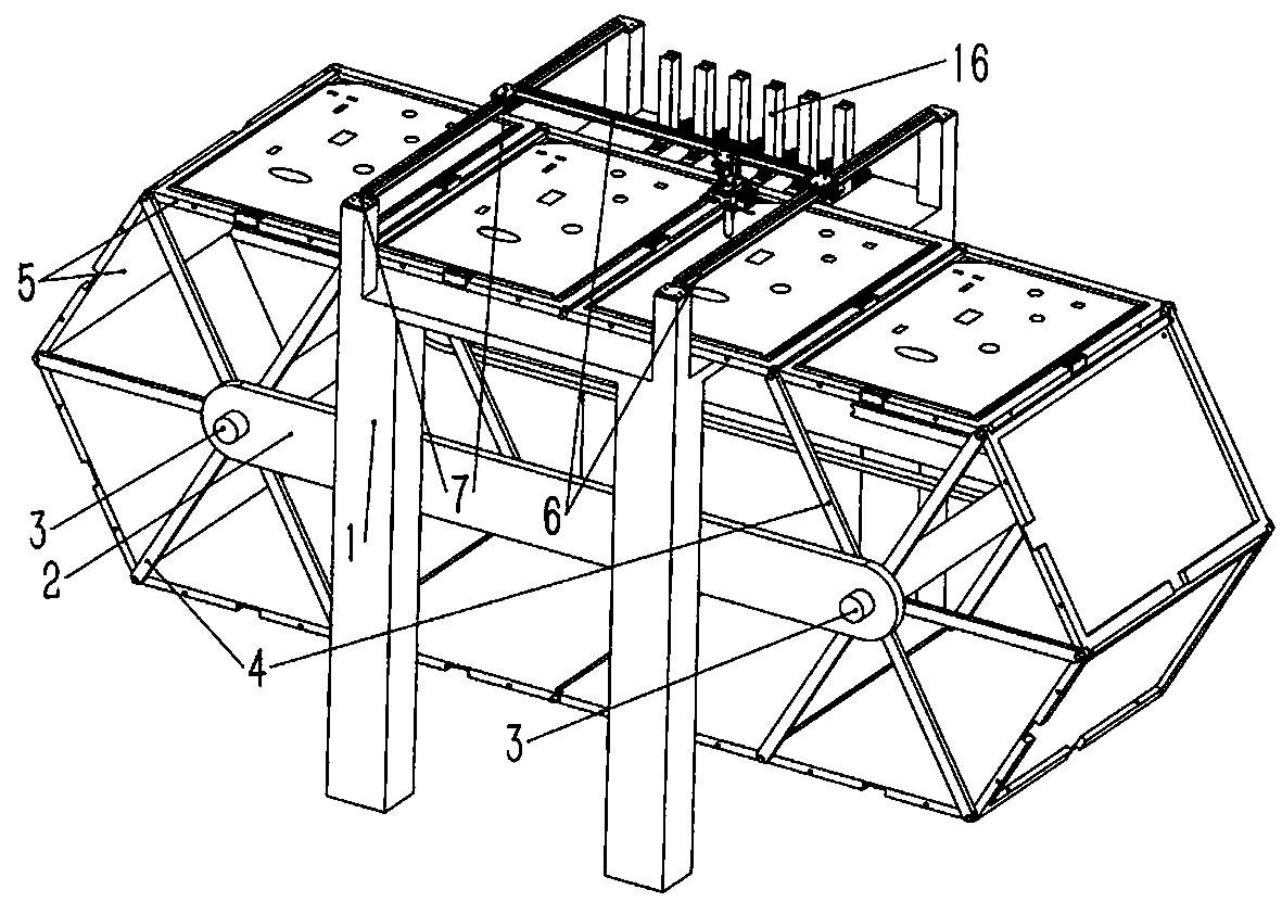
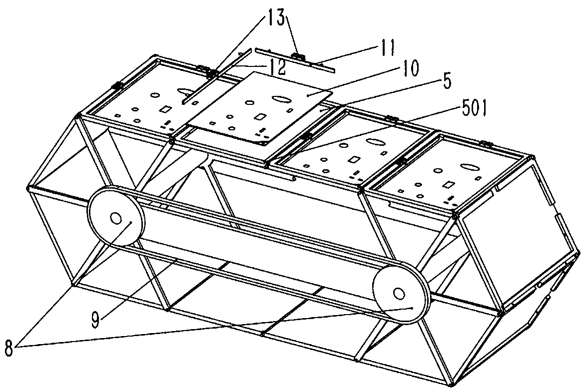
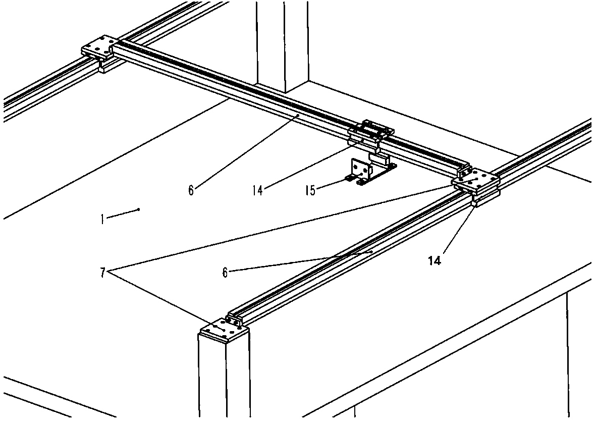
[0021] Example: such as Figure 1 to Figure 6 The semiconductor patch welding automatic layout equipment shown is a semiconductor patch welding automatic layout equipment, including a circuit board feeding module, a translation movement module, a patch feeding module and a patch picking and placing module, and its circuit The board feeding module also includes a chain-driven circular feeding mode, and the translation movement module also includes a screw guide rail-type feed driving mode.

[0022] The circuit board feeding module is designed for circular feeding, and has multiple stations including loading station, patch station, and unloading station, including two fixed plates 2 installed on the frame 1, of which , the rotating shaft 3 is installed on the two fixed plates 2, the bracket 4 is fixedly installed on the rotating shaft 3, the bracket 4 is designed with six arms, each arm has a semicircular groove at the top, and several loading plates 5 pass through the pin shaft...


PUM


Abstract

The invention discloses an automatic arrangement device for semiconductor patch welding. The automatic arrangement device is suitable to be used on a circuit board where semiconductor patches are automatically and accurately arranged during welding. The device provided by the invention can automatically identify, place and arrange the semiconductor patches, has the characteristics of high responseand high precision, can continuously operate, and can greatly improve the efficiency. The device employs a modular design, and comprises a circuit board feeding module, a motion module, a semiconductor patch feeding module and a patch taking and placing module, wherein all the modules work in a matched mode, so the use and maintenance are convenient and easy. The patch taking and placing module adopts an adhesive head to stick patches, so static electricity is avoided, the action is stable, the vibration is small, and the patch placing accuracy is kept to the maximum extent.

Description

technical field [0001] The invention provides an automatic arrangement device for semiconductor patch welding, which belongs to the design field of automatic arrangement equipment for semiconductor patch welding. Background technique [0002] The welding of semiconductor patches has always been a very delicate work. Whether it is manual placement or machine placement, it requires very high operational accuracy and stability. However, most of the existing manual placement, although experienced workers It can be placed very well, but the work is tiring. The labor intensity is very high; the cost of robot placement is very high, and it must be applied by medium and large enterprises. In view of the above reasons, it is a key point of the demand to design related simplified equipment, which can better complete the corresponding placement work, and the cost is low. Contents of the invention [0003] In view of the above current situation, the present invention provides an aut...

Claims


Application Information

Patent Timeline
Patent Type & Authority Patents(China)
IPC IPC(8): H05K13/04
CPCH05K13/043H05K13/0465
Inventor 滕吉美
Owner 台州市黄岩日隆模具厂(普通合伙)
Learn More