Supercharge Your Innovation With Domain-Expert AI Agents!

Welding machine transmission mechanism capable of transmitting large-sized silicon wafers

A transmission mechanism, large-scale technology, applied in the direction of conveyor objects, transportation and packaging, climate sustainability, etc., can solve the problems of inability to meet the transmission requirements of large-scale solar cells, unstable transmission, and low fragmentation rate, to avoid The effect of silicon wafer size deformation, reducing deformation and falling, and reducing fragmentation rate

Pending Publication Date: 2019-10-29
DONGFANG HUANSHENG PHOTOVOLTAIC (JIANGSU) CO LTD
View PDF0 Cites 0 Cited by
  • Summary
  • Abstract
  • Description
  • Claims
  • Application Information

AI Technical Summary

Problems solved by technology

[0002] As a renewable and environmentally friendly energy source, solar cells have attracted more and more attention, and the solar photovoltaic industry has also developed rapidly. With the increase in the demand for power generation by solar cells, the size of solar cells is getting larger and larger. The transmission structure cannot meet the transmission requirements of large-scale solar cells, with large deformation, unstable transmission, and low fragmentation rate

Method used


Image

  • Welding machine transmission mechanism capable of transmitting large-sized silicon wafers
  • Welding machine transmission mechanism capable of transmitting large-sized silicon wafers
  • Welding machine transmission mechanism capable of transmitting large-sized silicon wafers

Examples


Embodiment 1

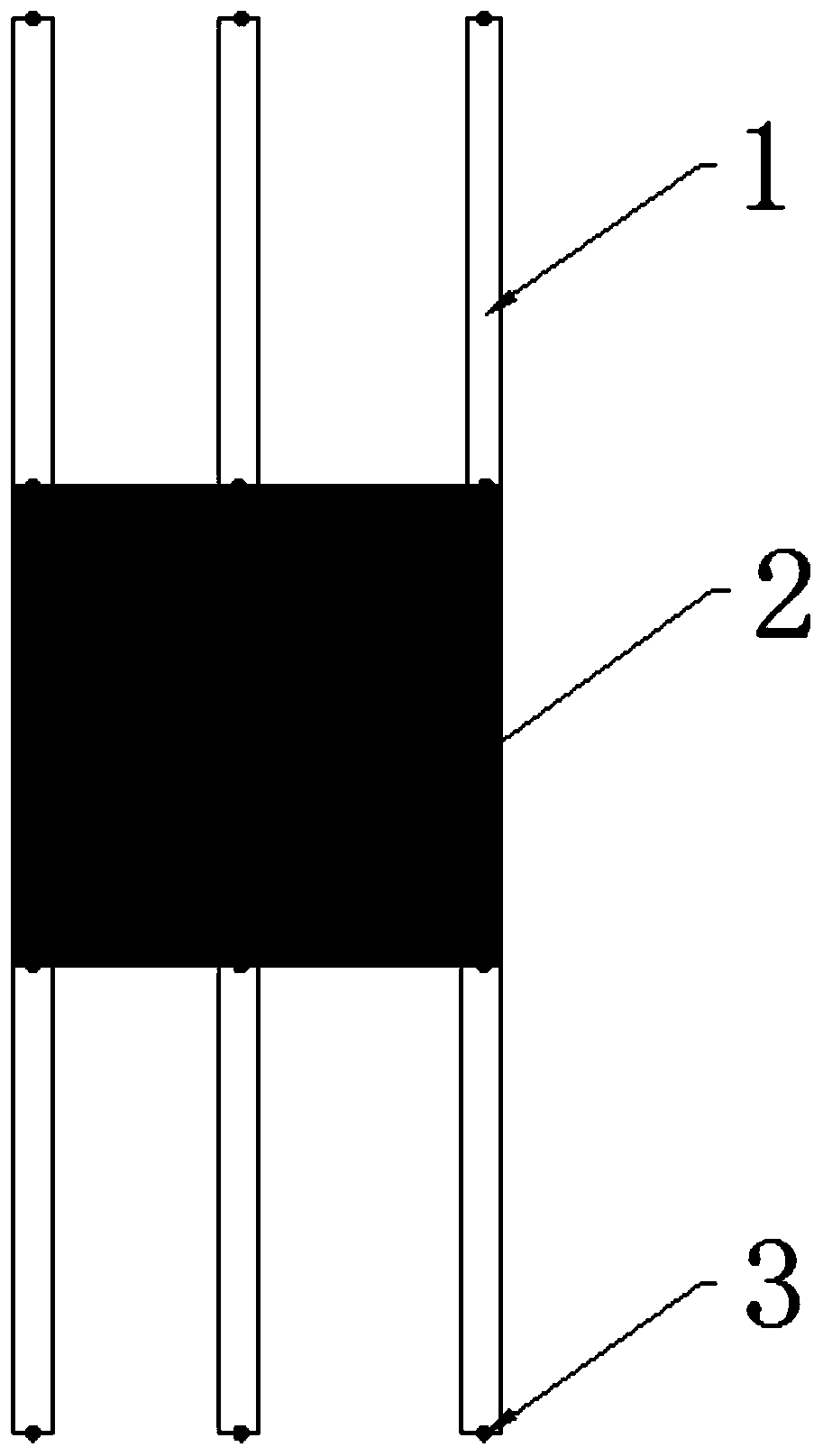
[0030] A welder transfer mechanism that can transfer large-size silicon wafers, such as figure 1 and image 3 As shown, it includes a transmission device and a positioning device 3, wherein the positioning device 3 is adjustable on the transmission device, the distance between adjacent positioning devices 3 can be adjusted, and the distance between adjacent positioning devices is the same as that of the silicon wafer 2 The size is adapted to facilitate the positioning and transmission of the silicon wafer 2. During the transmission process of the silicon wafer 2, the feeding sucker places the silicon wafer on the transmission device, and the silicon wafer 2 is placed between the adjacent positioning devices 3, and the silicon wafer 2 is positioned when it is transported on the transmission device, so as to avoid silicon The chip shakes, the precise positioning of the silicon chip is convenient for the loading sucker to load, realizes accurate loading and transportation, and a...

Embodiment 2

[0044] The difference between this embodiment and Embodiment 1 lies in the difference in the transmission structure, and the rest of the structures are the same. In this embodiment, the transmission structure will be described in detail, and the rest will not be repeated.

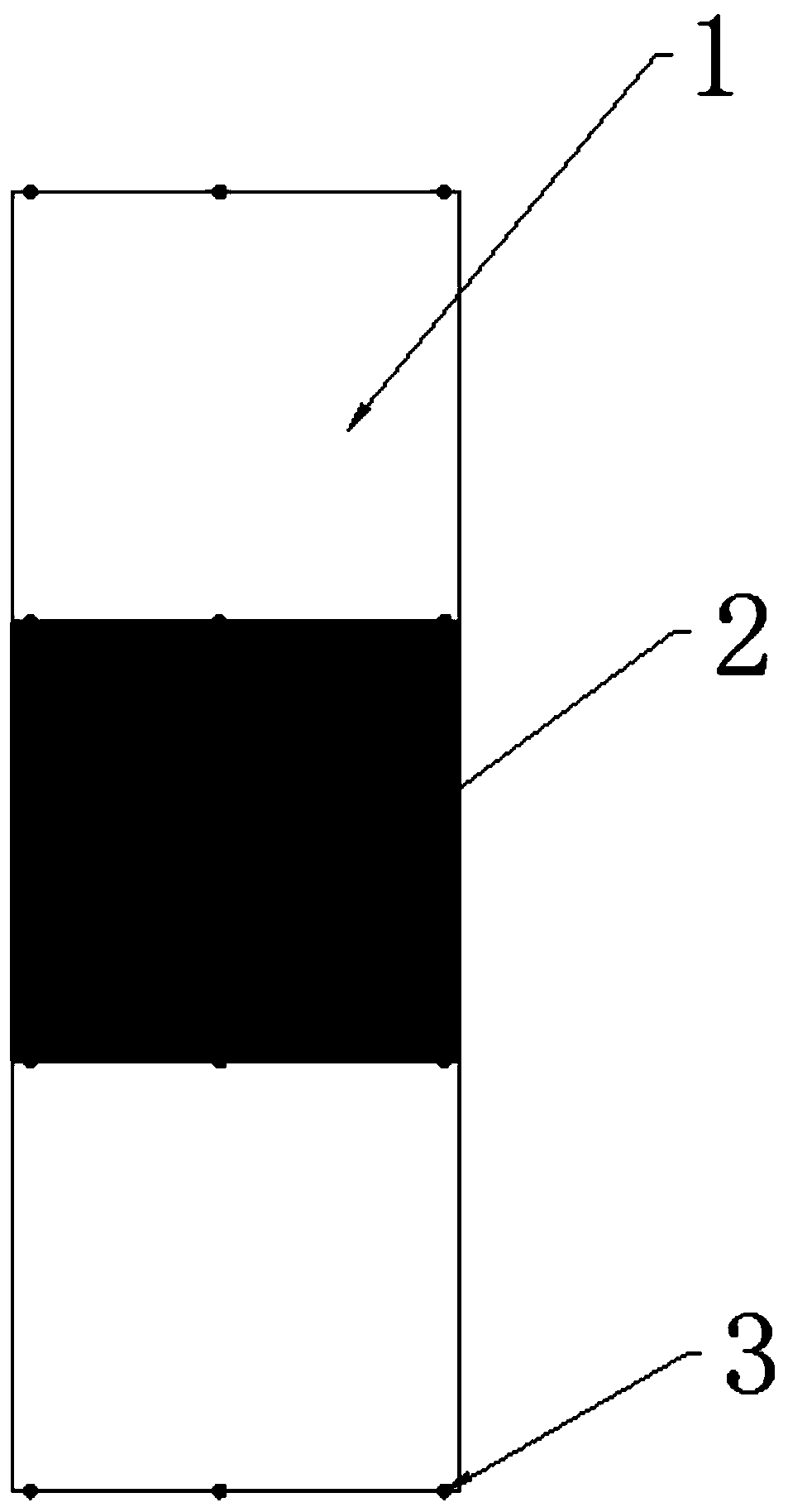
[0045] In this example, if figure 2As shown, the above-mentioned transmission device is a transmission belt 1, the width of the transmission belt 1 is greater than the width of the silicon wafer 2, the transmission belt 1 is a transmission belt 1 with a certain width, and the width of the transmission belt 1 is the same as the width of the silicon wafer 2 Compatible, easy to transport silicon wafers. A plurality of positioning devices 3 are installed at equal intervals on the conveyor belt 1, and the spacing is adapted to the size of the silicon wafer 2, which is convenient for feeding and transporting the silicon wafer 2; in the width direction of the conveyor belt 1, a positioning device is installed 3,...

Embodiment 3

[0048] The difference between this embodiment and Embodiment 1 and Embodiment 2 lies in the difference in the structure of the positioning device, and the rest of the structures are the same. In this embodiment, the structure of the positioning device will be described in detail, and the rest will not be repeated.

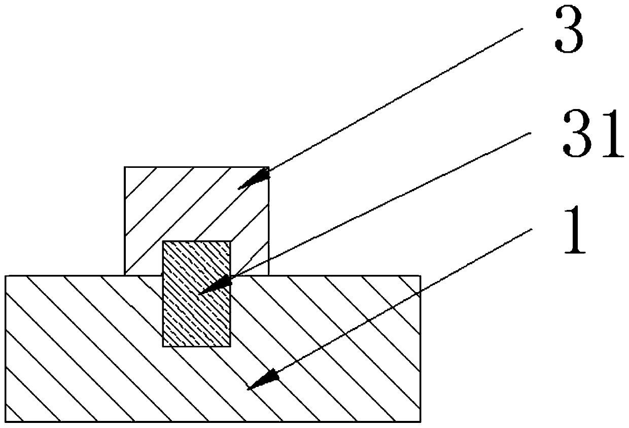
[0049] In this example, if Figure 4 As shown, the positioning device 3 is a positioning block, one end of the positioning block is equipped with a plug-in device 32, the free end of the plug-in device 32 is a tip, the plug-in device 32 is plugged on the conveyor belt 1, and the plug-in device The free end of 32 will not penetrate the transmission belt 1, and the positioning block is fixedly installed on the transmission belt 1. The plug-in device 32 is a pin, and the number of pins can be one, or two, or more One, select according to actual needs, no specific requirements are made here; use the plug-in device 32 to install the positioning blocks, so that the dista...


PUM


Abstract

The invention provides a welding machine transmission mechanism capable of transmitting large-sized silicon wafers. The welding machine transmission mechanism comprises a transmission device and positioning devices. The positioning devices are arranged on the transmission device. The distance between adjacent positioning devices is adapted to the size of silicon wafers, which is convenient for positioning and transmitting of silicon wafers. The welding machine transmission mechanism provided by the invention has the advantages that the positioning devices are provided to effectively ensure theposition and spacing of each silicon wafer and cooperate with the lateral support of a number of transmission belts or a wide transmission belt; size deformation of silicon wafers, which is caused byexcessive size of silicon wafers, can be avoided; silicon wafer deformation drop and transmission offset during transmission are reduced; and the fragmentation rate is reduced.

Description

technical field [0001] The invention belongs to the field of photovoltaic technology, and in particular relates to a welding machine transmission mechanism capable of transmitting large-size silicon wafers. Background technique [0002] As a renewable and environmentally friendly energy source, solar cells have attracted more and more attention, and the solar photovoltaic industry has also developed rapidly. With the increase in the demand for power generation by solar cells, the size of solar cells is getting larger and larger. The transmission structure cannot meet the transmission requirements of large-scale solar cells, with large deformation, unstable transmission, and low fragmentation rate. Contents of the invention [0003] In view of the above problems, the problem to be solved by the present invention is to provide a welding machine transmission mechanism that can transport large-size silicon wafers, especially suitable for the transmission of welding machines to...

Claims


Application Information

Patent Timeline
Patent Type & Authority Applications(China)
IPC IPC(8): H01L21/68H01L21/677H01L31/18
CPCH01L21/68H01L21/6776H01L31/1876Y02P70/50
Inventor 肖扬鑫桂军马擎天
Owner DONGFANG HUANSHENG PHOTOVOLTAIC (JIANGSU) CO LTD
Features
  • R&D
  • Intellectual Property
  • Life Sciences
  • Materials
  • Tech Scout
  • Unparalleled Data Quality
  • Higher Quality Content
  • 60% Fewer Hallucinations
Learn More