Planarization machining device and single-face and double-face planarization machining system

A processing device and flattening technology, which is applied in the direction of grinding devices, metal processing equipment, grinding tools, etc., can solve the problems of force distortion, low processing efficiency, lack of self-dressing of polishing pads and self-sharpening of abrasive materials, etc., to eliminate damage , Improve the effect of quality and efficiency

Active Publication Date: 2017-01-11
GUANGDONG NANOGRIND TECH CO LTD
View PDF5 Cites 13 Cited by
  • Summary
  • Abstract
  • Description
  • Claims
  • Application Information

AI Technical Summary

Problems solved by technology

[0003] A typical flattening processing technology of semiconductor substrate surface is classical magnetorheological finishing (Magnetorheological Finishing, MRF). Point-by-point scanning processing, but the processing efficiency is relatively low
In the cluster magnetorheological flattening processing method, the small-sized magnetic body used to form the magnetorheological effect polishing pad usually adopts a permanent magnet. During the processing, the gap between the workpiece and the polishing disc can only be adjusted Gap) to adjust the stiffness of the polishing disc. At the same time, the cluster magnetorheological effect polishing pad formed by the static magnetic field lacks the mechanism of self-dressing and self-sharpening of the abrasive. The viscoelasticity of the magnetorheological fluid under the action of the magnetic field makes the static magnetic field form The polishing pad is deformed by force on the surface of the workpiece after processing, and it is difficult to keep the performance of the processed workpiece stable, which restricts the further application and development of this process

Method used


Image

  • Planarization machining device and single-face and double-face planarization machining system
  • Planarization machining device and single-face and double-face planarization machining system
  • Planarization machining device and single-face and double-face planarization machining system

Examples


Embodiment Construction

[0038] The following will clearly and completely describe the technical solutions in the embodiments of the present invention with reference to the accompanying drawings in the embodiments of the present invention. Obviously, the described embodiments are only some, not all, embodiments of the present invention. Based on the embodiments of the present invention, all other embodiments obtained by persons of ordinary skill in the art without making creative efforts belong to the protection scope of the present invention.

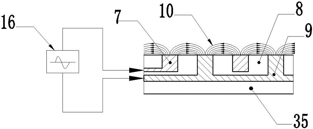
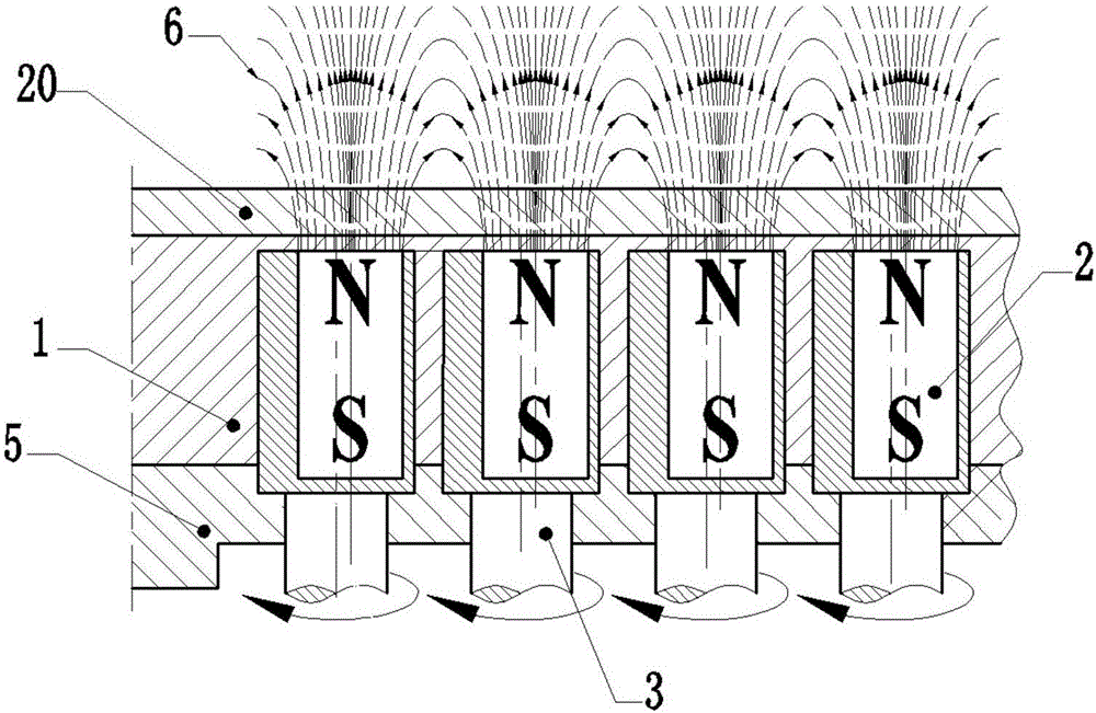
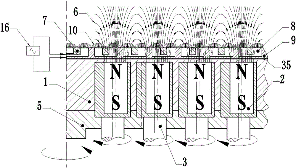
[0039] The core of the present invention is to provide a flattening processing device to improve the quality and efficiency of flattening processing on the workpiece surface. Another core of the present invention is to provide a single-side planarization processing system including the above-mentioned planarization processing device, so as to realize high quality and high efficiency in planarization processing of the workpiece surface. Another core of the pres...


PUM


Abstract

The invention discloses a planarization machining device and a single-face and double-face planarization machining system. The planarization machining device comprises a plurality of permanent magnets used for forming a multi-point self-rotation array magnetic pole, array positive electrodes, array negative electrodes and electromagnetic rheologic fluid; the end faces of the permanent magnets are arranged in a parallel and level manner in the same direction or in different directions; the permanent magnets are arranged in a magnetic pole installing disk through magnetic pole installing end covers; the permanent magnets are correspondingly arranged at the first end of a rotating shaft; a polishing disk is installed on the magnetic pole installing disk; the second end of the rotating shaft is connected with a magnetic pole synchronous rotating motor used for driving the permanent magnets to rotate synchronously and a transmission system; the array positive electrodes and the array negative electrodes are arranged on the polishing disk; the array positive electrodes, the array negative electrodes and the magnetic pole installing disk are arranged in a mutual insulation manner; the array positive electrodes and the array negative electrodes are connected with a low-frequency high-voltage square wave alternating power source; the electromagnetic rheologic fluid is arranged in the polishing disk and mixed with abrasive materials; and the electromagnetic rheologic fluid forms a polishing pad under the coupling action of a dynamic magnetic field and a low-frequency high-voltage square wave alternating electric field. By means of the device, the planarization machining quality and efficiency of the surface of a workpiece is improved.

Description

technical field [0001] The invention relates to the technical field of ultra-precision processing equipment, in particular to a flattening processing device applied to semiconductor substrates. In addition, the present invention also relates to a single-side planarization processing system including the above-mentioned planarization processing device and a double-side planarization processing system including the above-mentioned planarization processing device, which are applied to semiconductor substrates. Background technique [0002] With the rapid development of microelectronics and optoelectronics technology, new-generation semiconductor substrates such as single crystal SiC, sapphire, and glass substrates are developing in the direction of large size and ultra-thinning, and the processing requirements for semiconductor substrates are also getting higher and higher. Not only The wafer is required to achieve sub-nanometer surface roughness, and the wafer is also required...

Claims


Application Information

Patent Timeline
Patent Type & Authority Applications(China)
IPC IPC(8): B24B37/07B24B37/20B24B37/34
CPCB24B37/07B24B37/20B24B37/34
Inventor 阎秋生潘继生
Owner GUANGDONG NANOGRIND TECH CO LTD
Why Eureka
Try Eureka