Flat panel detector and manufacturing method thereof

A flat-panel detector and manufacturing method technology, applied in the direction of final product manufacturing, sustainable manufacturing/processing, semiconductor devices, etc., can solve the problems of reducing the detection sensitivity of photodetectors, failure of TFT devices, and increase of TFT leakage current

Active Publication Date: 2019-10-29
NANJING DETECH FUTURE TECH CO LTD
View PDF4 Cites 5 Cited by
  • Summary
  • Abstract
  • Description
  • Claims
  • Application Information

AI Technical Summary

Problems solved by technology

In the process of making the photoelectric conversion layer 90, a large amount of hydrogen gas is needed. If the hydrogen ions diffuse into the semiconductor layer 30, in severe cases, the TFT device will fail.
[0005] The flat-panel detector needs to place the detection panel

Method used


Image

  • Flat panel detector and manufacturing method thereof
  • Flat panel detector and manufacturing method thereof
  • Flat panel detector and manufacturing method thereof

Examples


Embodiment Construction

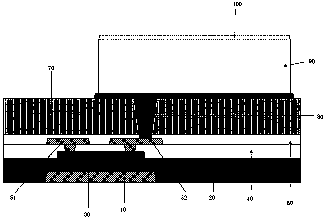
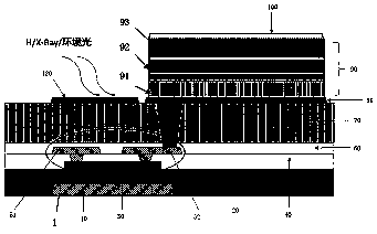
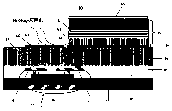
[0048] Below in conjunction with accompanying drawing and specific embodiment, further illustrate the present invention, should be understood that these embodiments are only for illustrating the present invention and are not intended to limit the scope of the present invention, after having read the present invention, those skilled in the art will understand various aspects of the present invention Modifications in equivalent forms all fall within the scope defined by the appended claims of this application.

[0049] In order to make the drawing concise, each drawing only schematically shows the parts related to the present invention, and they do not represent the actual structure of the product. In addition, to make the drawings concise and easy to understand, in some drawings, only one of the components having the same structure or function is schematically shown, or only one of them is marked. Herein, "a" not only means "only one", but also means "more than one".

[0050] ...


PUM


Abstract

The invention provides a flat panel detector and a manufacturing method thereof. The flat panel detector comprises a TFT device with a semiconductor layer, a first insulating layer covering the TFT device, an interlayer insulating layer on the first insulating layer, a cathode electrode which is located on the interlayer insulating layer and connected with the TFT device, and a photoelectric conversion layer located on the cathode electrode. The flat panel detector further comprises a barrier layer on the interlayer insulating layer. At least part of the barrier layer is in a floating state, and at least part of the barrier layer is located directly above the semiconductor layer. According to the invention, the barrier layer is arranged on the flat panel detector; at least part of the barrier layer is located directly above the semiconductor layer; and the barrier layer can block the influence of hydrogen diffusion on the semiconductor layer when the photoelectric conversion layer is formed, and can block the influence of X-ray or ambient light on the semiconductor layer.

Description

technical field [0001] The present invention relates to the technical field of flat panel detectors, in particular to a flat panel detector and a manufacturing method thereof. Background technique [0002] The X-ray of the flat-panel detector is first converted into visible light by the fluorescent medium material, and then the visible light signal is converted into an electrical signal by the photosensitive element, and finally the analog electrical signal is converted into a digital signal by A / D. [0003] Such as figure 1 As shown, the flat panel detector includes a gate 10, a gate insulating layer 20 covering the gate 10, a semiconductor layer 30 on the gate insulating layer 20, an etching barrier layer 40 covering the semiconductor layer 30, and an etching barrier layer passing through the gate insulating layer 20. The source electrode 51 and the drain electrode 52 of the layer 40 are both in contact with the semiconductor layer 30, the first insulating layer 60 coveri...

Claims


Application Information

Patent Timeline
IPC IPC(8): H01L31/0352H01L31/115H01L31/18
CPCH01L31/0352H01L31/115H01L31/18Y02P70/50
Inventor 陈钢
Owner NANJING DETECH FUTURE TECH CO LTD
Why Eureka
Try Eureka