Substrate integrated waveguide adjustable filter
A substrate-integrated waveguide and half-mode substrate-integrated technology, applied in the field of radio frequency, can solve the problems of complex installation and large volume, and achieve the effects of low processing cost, small volume, and simple realization.
- Summary
- Abstract
- Description
- Claims
- Application Information
AI Technical Summary
Problems solved by technology
Method used
Image
Examples
Embodiment 1
[0041] This embodiment provides a substrate-integrated waveguide tunable filter. It includes: a dielectric substrate; a first metal layer disposed on the dielectric substrate and a second metal layer disposed below the dielectric substrate; distributed on the edge of the first metal layer and penetrating A plurality of first metallized through holes of the first metal layer, the dielectric substrate and the second metal layer; at least one unmetallized trench penetrating through the first metal layer and the dielectric substrate; And, corresponding to at least one tuning device embedded in the unmetallized trench, the position of the tuning device in the trench is adjustable.
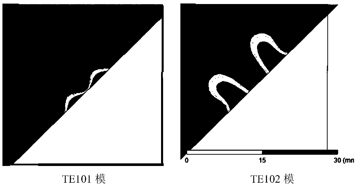
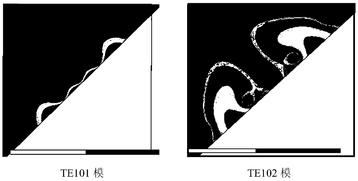
[0042] The substrate-integrated waveguide tunable filter of this embodiment utilizes the movement of the tuning device in the unmetallized trench to disturb the electromagnetic field distribution and realize the adjustable resonance frequency. After the tuning device moves to a specific position, a spec...
Embodiment 2
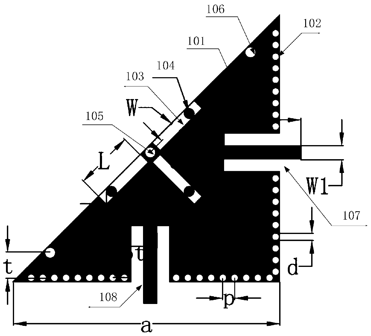
[0044] This embodiment is a further description of Embodiment 1. figure 1 The specific structure of a substrate-integrated waveguide tunable filter of this embodiment is shown. The substrate-integrated waveguide tunable filter is a half-mode substrate-integrated waveguide tunable filter, which includes a dielectric substrate (not shown in the figure), a first metal layer 101, a second metal layer (not shown in the figure) out), several first metallized vias 102, three unmetallized trenches 103 and three tuning devices 104.
[0045] The first metal layer 101 is disposed on the dielectric substrate. The second metal layer is disposed under the dielectric substrate. In this embodiment, the first metal layer 101 is a right-angled triangle (such as an isosceles right-angled triangle with a side length a), and the dielectric substrate and the second metal layer can be The layers 101 are triangles with the same size, squares with side length a or slightly larger than a, or other s...
Embodiment 3
[0056] This embodiment is basically the same as Embodiment 2, the difference is that, as Figure 5 As shown, the substrate integrated waveguide tunable filter of this embodiment may include two unmetallized trenches 103 and two tuning devices 104, the angle between the two unmetallized trenches 103 is 180°, can be seen as omitting figure 1 The unmetallized trench in the middle. The tunable principle of the substrate-integrated waveguide tunable filter is the same as that of Embodiment 2. The size of each part in the filter can be obtained through simulation design according to a specific center frequency.
PUM
| Property | Measurement | Unit |
|---|---|---|
| thickness | aaaaa | aaaaa |
Abstract
Description
Claims
Application Information


