Thin film surface defect detection method, system and equipment based on deep learning

A deep learning and defect detection technology, applied in the field of film surface defect detection based on deep learning, can solve the problems of high labor intensity, complex deployment and high cost, and achieve the effects of high repeatability, simple deployment and high accuracy.

Active Publication Date: 2019-11-19
上海深视信息科技有限公司
View PDF10 Cites 10 Cited by
  • Summary
  • Abstract
  • Description
  • Claims
  • Application Information

AI Technical Summary

Problems solved by technology

In the assembly line production process, due to vibration, air flow and other reasons, various types of defects will occur on the surface of the optical film, such as scratches, indentations, corners, pits, black spots, black spots, white spots, wrinkles, bubbles and foreign matter, etc., leading to a decline in the use effect of the product
[0003] In the field of traditional optical film production, due to the optical properties of optical films, it is difficult to image and identify various defects, which makes it difficult to realize automatic monitoring. Most optical films can only be detected by manual visual inspection, but this detection method On the one hand, it is easily affected by subjective judgments, resulting in unstable test results and poor reliability. On the other hand, it is labor-intensive and costly, making it difficult to meet the needs of mass production
However, those that can realize automatic detection can only detect a small number of types of defects, and cannot detect all defects at the same time. The deployment is complicated and the repeatability is poor.

Method used


Image

  • Thin film surface defect detection method, system and equipment based on deep learning
  • Thin film surface defect detection method, system and equipment based on deep learning

Examples


Embodiment Construction

[0029] The following will clearly and completely describe the technical solutions in the embodiments of the present invention with reference to the accompanying drawings in the embodiments of the present invention. Obviously, the described embodiments are only some, not all, embodiments of the present invention. Based on the embodiments of the present invention, all other embodiments obtained by persons of ordinary skill in the art without creative efforts fall within the protection scope of the present invention.

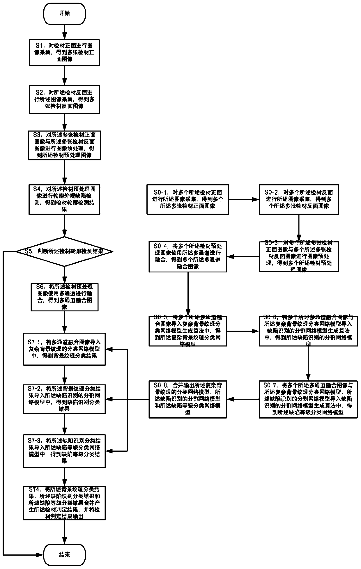
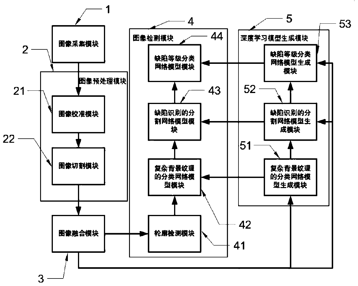
[0030] In a specific embodiment, such as figure 1As shown, a film surface defect detection method based on deep learning includes: S1: collect images on the front side of the inspection material to obtain multiple front images of the inspection material; S2: collect images on the back side of the inspection material to obtain multiple images of the inspection material Reverse image; S3: Perform image preprocessing on multiple front images of the inspection material...


PUM


Abstract

The invention provides a film surface defect detection method, system and equipment based on deep learning. The film surface defect detection method based on deep learning comprises the steps: S1, conducting image acquisition on the front face of a detected material; S2, carrying out image acquisition on the reverse side of the detected material; S3, performing image preprocessing; S4, carrying out contour appearance defect detection; S5, judging a contour detection result; S6, performing fusion by using multiple channels to obtain a multi-channel fusion image; and S7, importing into a pre-trained deep learning model. The film surface defect detection system based on deep learning comprises an image acquisition module, an image preprocessing module, an image fusion module and an image detection module, thin film surface defect detection equipment based on deep learning comprises a memory and a processor. The method has the beneficial effects that the defects of the optical thin film can be effectively identified on the premise of low cost, the labor cost is reduced, the identification efficiency is improved, the deployment is simple, and the repeatability is higher.

Description

technical field [0001] The invention relates to the field of optical thin film detection, in particular to a method, system and equipment for detecting defects on the surface of thin films based on deep learning. Background technique [0002] Optical thin films are widely used in liquid crystal displays of mobile phones, computers, and televisions, glasses coatings, solar panels, and other fields. Optical films are composed of thin layered media through which light beams propagate, mainly including reflective films, anti-reflective films, filter films, optical protective films, polarizing films, etc., which have extremely high requirements for surface quality. In the assembly line production process, due to vibration, air flow and other reasons, various types of defects will occur on the surface of the optical film, such as scratches, indentations, corners, pits, black spots, black spots, white spots, wrinkles, bubbles and foreign matter, etc., leading to a decline in the u...

Claims


Application Information

Patent Timeline
Patent Type & Authority Applications(China)
IPC IPC(8): G06T7/00G06K9/62G06N20/00
CPCG06T7/0004G06N20/00G06F18/253G06F18/214
Inventor 毛雪慧陈果闫龑王洋
Owner 上海深视信息科技有限公司
Why Eureka
Try Eureka