
Chemical fine resistance adjusting method and etchant for resistor embedded in nickel-phosphorus layer

A technology for burying resistors and nickel-phosphorus layers, applied in resistors, resistor manufacturing, coating resistor materials, etc., can solve the problems of thickness variation, small target value, and influence of buried resistor layers, achieve uniform corrosion, and improve control accuracy. Effect

Active Publication Date: 2019-11-19
BOMIN ELECTRONICS CO LTD
View PDF7 Cites 2 Cited by
  • Summary
  • Abstract
  • Description
  • Claims
  • Application Information

AI Technical Summary

Problems solved by technology

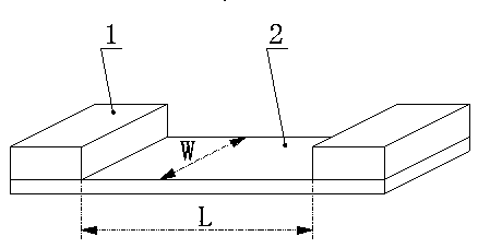
[0006] However, after the buried resistance circuit is formed, the circuit board still needs to undergo subsequent processes such as solder resistance and surface treatment. In the pre-treatment of the subsequent process, the buried resistance layer (nickel-phosphorus alloy layer) is often corroded, resulting in changes in the thickness of the buried resistance layer. The impact on the resistance value is not as precise and controllable as the pattern etching process, which often leads to the resistance value of the board after the pre-soldering treatment is smaller than the design target value; in view of the above-mentioned problem of small resistance value, the existing control method or through laser Ablating part of the copper foil in contact with the square buried resistance, or re-ablating a compensated buried resistance pattern around the hole by laser, there is a problem that the laser ablation of the copper surface will affect the nickel-phosphorus alloy layer. These are fine Obstacles to uniformly adjust the resistance value, causing the adjusted resistance value to fail to meet expectations, which is unacceptable for buried resistance circuit board products with high resistance requirements

Method used


Image

  • Chemical fine resistance adjusting method and etchant for resistor embedded in nickel-phosphorus layer
  • Chemical fine resistance adjusting method and etchant for resistor embedded in nickel-phosphorus layer
  • Chemical fine resistance adjusting method and etchant for resistor embedded in nickel-phosphorus layer

Examples


Embodiment Construction

[0033] The present invention will be further described below in conjunction with the specific embodiments in the accompanying drawings.

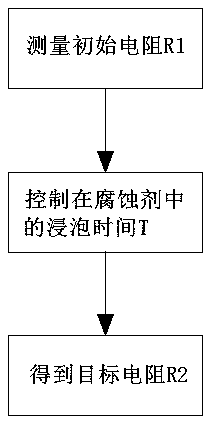
[0034] refer to image 3 , a method for chemically fine-tuning the resistance of a nickel-phosphorus layer embedded resistance. First, measure the initial resistance value R1 of the resistance before the resistance adjustment, and obtain the target resistance of the resistance by controlling the immersion time T of the resistance in the etchant used to corrode the nickel-phosphorus alloy layer. Value R2. The working temperature of the etchant is 50-90°C, preferably, the working temperature of the etchant is 65°C, the activity of the etchant is high, and the corrosion is fast and stable.


PUM


Abstract

The invention discloses a chemical fine resistance adjusting method for a resistor embedded in a nickel-phosphorus layer, and belongs to the technical field of circuit boards. The method mainly solvesthe technical problem that a conventional resistance adjusting method cannot finely and uniformly adjust a resistance value. The method comprises firstly measuring the initial resistance value R1 ofa resistor before resistance adjustment; and obtaining the target resistance value R2 of the resistor by controlling the immersion time T of the resistor in an etchant for etching a nickel-phosphorusalloy layer. The invention discloses a chemical fine resistance adjusting etchant for a resistor embedded in a nickel-phosphorus layer. The method etches the nickel-phosphorus alloy layer uniformly, and can finely control the change of the resistance by controlling the time so as to obtain the target resistance value and improve the resistance control precision.

Description

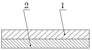
technical field [0001] The invention relates to the technical field of circuit boards, and more specifically relates to a method for chemically fine-tuning resistance embedded in a nickel-phosphorus layer and an etchant. Background technique [0002] As a method to replace the surface resistor patch, the PCB embedded resistance process can save the increasingly tight surface space of the PCB, and it is also more reliable than the chip resistor. Using nickel-phosphorus alloy buried resistance copper foil is one of the realization methods of buried resistance board. [0003] Nickel-phosphorus alloy buried resistance copper foil refers to a special copper foil material made by sputtering or electroplating a layer of nickel-phosphorus alloy 2 on the copper foil 1. Its structure is as figure 1 shown. Among them, the thickness of the nickel-phosphorus alloy material is mostly controlled at 0.1 μm to 0.4 μm. [0004] A nickel-phosphorus alloy buried resistance plate is formed b...

Claims


Application Information

Patent Timeline
IPC IPC(8): H01C17/00H01C17/14C23F1/18
CPCC23F1/18H01C17/00H01C17/003H01C17/14
Inventor 梁鸿飞陈世金徐缓韩志伟许伟廉郭茂桂陈苑明张胜涛
Owner BOMIN ELECTRONICS CO LTD
Learn More